Debounce + latch using inverters

Thread Starter

hrs

Joined Jun 13, 2014
525
Hi,

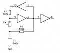
I found the attached circuits somewhere once. I get how it works, but suppose you hold the button longer than you should then the capacitor voltage will tend to mid-rail where it will be more sensitive to bouncing once you let go or may end up switching the inverter with input 3 if you hold it indefinitely.

When I make R1 equal to 10k the circuit appears to be better behaved in a sim. If you make R1 too small the current spikes through R1 might get bigger than you'd like(?) so don't make it too small but other than that is there a reason for R1 to be as large a value as R2?

Thanks
 

Attachments

Thread Starter

hrs

Joined Jun 13, 2014
525
Ok, so I think the original circuit would not be suitable for a CD4069 and R1 would indeed need to be lower value than R2. But it (the original circuit) would be fine for a CD40106 though it wouldn't hurt in this case for R1 to be a lower value.
 

nsaspook

Joined Aug 27, 2009
16,275
Ok, so I think the original circuit would not be suitable for a CD4069 and R1 would indeed need to be lower value than R2. But it (the original circuit) would be fine for a CD40106 though it wouldn't hurt in this case for R1 to be a lower value.
When I need serious debouncing with zero issues I use a dedicated chip.
https://www.analog.com/en/products/max812.html
1742420181423.png


https://www.analog.com/media/en/technical-documentation/data-sheets/max6816-max6818.pdf
1742420742586.png
The MAX6818 octal switch debouncer is designed for data-bus interfacing. The MAX6818 monitors switches and provides a switch change-of-state output (CH), simplifying microprocessor (µP) polling and interrupts. Additionally, the MAX6818 has three-state outputs controlled by an enable (EN) pin, and is pin-compatible with the LS573 octal latch (except for the CH pin), allowing easy interfacing to a digital data bus.
https://www.ti.com/lit/ds/symlink/tic12400.pdf?ts=1742372388576
1742421419292.png
The TIC12400 is an advanced Multiple Switch Detection Interface (MSDI) device designed to detect external switch statuses. The TIC12400 supports 24 direct inputs, with 10 inputs configurable to monitor digital I/O switches. 6 wetting current settings can be programmed for each input to support different application scenarios. The TIC12400 features an integrated 10-bit ADC to monitor multi-position analog switches and a comparator to monitor digital switches independently of the MCU. The device supports wake-up operation on all switch inputs to eliminate the need to keep the MCU active continuously, thus reducing power consumption of the system. The TIC12400 supports 2 modes of operations: continuous and polling mode. In continuous mode, wetting current is supplied continuously. In polling mode, wetting current is turned on periodically to sample the input status based on a programmable timer, thus the system power consumption is significantly reduced. The TIC12400 also offers various fault detection and diagnostic features for improved system robustness.
 
Last edited:

Ian0

Joined Aug 7, 2020
13,118
I always used R1=10k and R2=1M
And it only needs two inverters not three, because you can take the final output from pin 2. The pin 5/pin 6 inverter is redundant.
If you use a 4001 nor gate you can reset it from an external input.
 

nsaspook

Joined Aug 27, 2009
16,275
How much? You can buy an awful lot of Rs and Cs for £9.34.
The chips (with interrupt on change output tri-state latches) are on a interrupt event driven data bus that can easily handle more than 200 debouncers of 8 switches each on machines that cost millions. The TIC12400 has a SPI interface for 24 switches on device select pin with controls for sinking or sourcing wetting currents (https://en.wikipedia.org/wiki/Wetting_current) and fault testing.

It's a different engineering design world (24/7 for decades in harsh electrical environments) than simple Rs and Cs.
 
Last edited:

Thread Starter

hrs

Joined Jun 13, 2014
525
I always used R1=10k and R2=1M
Regardless of whether you use a Schmitt trigger inverter or not?
And it only needs two inverters not three, because you can take the final output from pin 2. The pin 5/pin 6 inverter is redundant.
Ah, I see what you mean. I didn't put much thought into it but assumed it buffered node 4. But it's entirely redundant.

That will make it even more difficult for my inner autist to deal with not 3 but 4 unused gates. If only there was 2 or 3 gate package that could withstand high-ish voltages. I see there are some for 5V. I think the scheme from post #1 will be the smallest foot print / lowest number of parts barring a dedicated chip, at least that I have found so far.
 

nsaspook

Joined Aug 27, 2009
16,275

Thread Starter

hrs

Joined Jun 13, 2014
525
Thanks, I'll have a look.

Looking for inverters I came across the CD40107 which seems to be a rare DIP8 exception. Maybe I can noodle out a way to make an SR-latch work with a push button.
 

Ian0

Joined Aug 7, 2020
13,118
Regardless of whether you use a Schmitt trigger inverter or not?

Ah, I see what you mean. I didn't put much thought into it but assumed it buffered node 4. But it's entirely redundant.

That will make it even more difficult for my inner autist to deal with not 3 but 4 unused gates. If only there was 2 or 3 gate package that could withstand high-ish voltages. I see there are some for 5V. I think the scheme from post #1 will be the smallest foot print / lowest number of parts barring a dedicated chip, at least that I have found so far.
You'll have to dream up a purpose for two more switch inputs! Then it will fully use the package.
(Or one more switch if you use a 4001)
If you want it to work at 5V then there is the 74LVC2G04 or 74LVC2G14
 
Top