AC/DC Inverters

tom66

Joined May 9, 2009
2,595
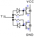
I'm talking about your circuit diagram. It mentions NPN and PNP transistors.

For the MOSFETs, any high power complementary pair will do. Usually you'll want MOSFETs of the same family.

Depends on how much power you are going to be using, and how much heat and efficiency you are willing to sacrifice for price, size, package, heatsink, etc.

If you want say 120W output power, given 80% efficiency, you will need 150W, which is 12.5 amps.

The IRF9530 P-channel has a 0.2 ohm Rds(on), which is quite high; it's rated for 14A. At the given 12.5 amps, it dissipates 31.25 watts approximately. This is below its package rating of 79 watts. A good heatsink WILL be required or the MOSFET will burn in seconds. This is not taking into account the switching dissipation, but if it's a 50Hz or 60Hz signal, that will be small, I think.

I mention this MOSFET because I am familiar with it and have a few spare...

Anyone know what the complementary of the IRF9530 is?
 

Thread Starter

Wendy

Joined Mar 24, 2008
23,429
Take a look at either the article of the bottom diagram of post #17, they've been replaced.

I don't think (but also don't know) that MOSFETs come in complimentary flavors. I have a fair stock of several types, but I'm interested what people consider the more common parts.
 

tom66

Joined May 9, 2009
2,595
You do generally get MOSFETs in complementary flavours. Because you deal with push-pull converters in inverters and DC-DC converters, as you show in your circuit. You usually have a high-side and a low-side MOSFET, and you must have appropriate gate driving circuitry for it to work.

That's what I understand.
 

Thread Starter

Wendy

Joined Mar 24, 2008
23,429
Most H Bridge circuits I have seen use the same flavor MOSFET (n channel). A while back I had a thread I started asking how to do this, basically there is a circuit that will charge a capacitor to keep the circuit on for that cycle.

High Side MOSFET Drivers
 

SgtWookie

Joined Jul 17, 2007
22,230
Mixing N-ch and P-ch MOSFETs in an H-bridge is OK for hobbyist-type circuits that are low frequency, as the drive requirements are more easily met.

If you want a true P-ch complement to an N-ch MOSFET, your total gate charge will suffer quite a bit, and you'll need about double the charge current on the P-ch MOSFETs as the N-ch's.

That's why the more serious H-bridge circuits use N-ch MOSFETs all around, and have high-side gate drivers that exceed Vcc/V+ by 10v to 15v; there's usually a boost capacitor with it's negative terminal tied to the source terminal of the high-side MOSFET; when the voltage on the source terminal rises, the charge on the cap rises right along with it.

Many of these boost-cap scheme drivers have to be cycled frequently in order to re-charge the boost cap. There are also high-side drivers that have built-in charge pumps to keep the high side caps charged offered by various manufacturers; this type can have the high side MOSFET on indefinitely. They're more expensive, of course.
 

SgtWookie

Joined Jul 17, 2007
22,230
Bill,
I'm not certain what schematic you are referring to.

If you are talking about a complete H-bridge configuration with an inductor/coil connected across it, then no - the coil will have nothing to do with shoot-through.

Shoot-through occurs when both the high and low side MOSFETs on the left or right of an H-bridge occur at the same time. Basically, it's a dead short across the supply, which usually causes smoke and unpleasant odors.

This schematic:


...from the thread you referenced: http://forum.allaboutcircuits.com/showpost.php?p=209559&postcount=4

... has the problem of propagation delay via the inverters, and no "dead time". "Dead time" is the delay between when the high/low side MOSFETs begin the process of being turned off, before the low/high side MOSFETs are allowed to start turning ON.

It takes time to charge/discharge a MOSFET gate. Then after they are charged/discharged, it takes them awhile to turn ON/OFF. Then you add a "finagle factor" to make certain that the dreaded shoot-thru won't happen. If it does, you will know right away by the sudden appearance of a miniature fireball accompanied by a loud ((<<**BANG**>>)) on your test bench with smoke, and an acrid yet familiar smell.

While you're first experimenting with these things, give yourself plenty of finagle factor. Then use your dual-trace scope to see how well your calculations stack up to "the real deal" in bench testing. Don't forget that your scope probes will add capacitive loading to the gate signal; if you're running close on dead time, that can push you over the edge. You can see the signal without actually touching the gate node by holding your probe tip just above the trace/wire. You'll get a little bit of capacitive coupling. It won't be much, so you'll have to crank up your V/div. However, you'll only add a pF or two to the gate charge requirement.
 

Thread Starter

Wendy

Joined Mar 24, 2008
23,429
This one...


For the sake of argument I'm moving on, assuming these will work. I am still interested in other ideas though. I can always come back and edit the post.
 
Last edited:

SgtWookie

Joined Jul 17, 2007
22,230
You don't want to do that. Inductors are relatively expensive (copper) and bulky.

CRn is an archaic reference designator. While historically interesting, please keep in mind that this is potentially confusing for n00bs, which we are attempting to mentor. "CR" stands for "Crystal Rectifier", from back in the days when germanium diodes were all the rage. Unless your circuit actually requires a germanium diode, please use the more modern reference designator of "Dn", where a silicon or Schottky diode is indicated.

I am not certain offhand what the purpose of L1 is supposed to be, as the transformer will be at least 10mH, likely much more. If one wanted to suppress transients in the MHz range, that would be one way to do it, which may have been the intent.

C4 will likely explode pretty quickly. There will be quite a bit of power dissipation in it.

If you want to fuse something, use a 1/4A fuse on the 555 side, and then use a 10A fuse on the entire half-H bridge. That way you might blow a $1 fuse instead of a $0.50 MOSFET.

Would you believe that I have a collection of mil-spec fuses that are over 30 years old?
[eta]
I just pulled out a cardboard 5-pack. They're labeled:
Rich (BB code):
5920-727-1452 (that's the NSN, or National Stock Number)
FUSE, 
F03B 32V 10A
5 EACH
DSA900-69-C-4553
A        3/69
I was a freshman in HS then.
The end caps seem to be nearly as shiny as the day they were made. The center body is ceramic. They were made by Buss Fuse.
 
Last edited:

Thread Starter

Wendy

Joined Mar 24, 2008
23,429
The idea was to prevent shoot through. L2 and L3 is meant to slow turn on. 1µH may not be enough to cover potential shoot through I think. The transition speed is very fast, so it might work as is.

The cap is left over from Tony's circuit (Figure 1). So you think it would blow with 10 amps flowing through it? What do you suggest, paralleling several caps (4 or 5 might do it)?

If I wanted to protect the MOSFETs I would have to have a fuse for each MOSFET. The fuse shown is to protect the output from overload, I could use a 1A on the 120VAC like I did for Figure 2.
 

SgtWookie

Joined Jul 17, 2007
22,230
The idea was to prevent shoot through. L2 and L3 is meant to slow turn on. 1µH may not be enough to cover potential shoot through I think. The transition speed is very fast, so it might work as is.
You are opening a rather large can of worms trying to use inductors to control shoot-through. It's usually done at a logic level using RC time. The gates have disable logic that the dead time controls.

The cap is left over from Tony's circuit (Figure 1). So you think it would blow with 10 amps flowing through it? What do you suggest, paralleling several caps (4 or 5 might do it)?
It's a rather weak attempt at a push-pull type circuit. Tony was attempting to stop the flux walking by using a capacitor (or several capacitors).

I'm not going to try to "fix" this circuit. It would be much easier to start completely fresh.

If I wanted to protect the MOSFETs I would have to have a fuse for each MOSFET. The fuse shown is to protect the output from overload, I could use a 1A on the 120VAC like I did for Figure 2.
No, just a single 10A fuse in the line between 12V and the MOSFET half-bridge would keep it from getting fried very often.
 

timrobbins

Joined Aug 29, 2009
318
Some design considerations are (for the sake of design discussion, rather than to promote an improved circuit per se):

Cross-conduction (aka shoot through) can be alleviated by using an asymetric diode resistor driver to lengthen the turn-on times, and shorten the turn-off times. Gate capacitance can be used to normalise the transition times, and improve protection of gate. Another method to consider is zeners to each gate to level shift the voltage from the 555 needed to turn each fet on. This method has the disadvantage of reducing the enhancement voltage, and being influenced by rail voltage.

The anti-parallel diode in each FET will do a good job at clamping over/under voltages on the midpoint to either pos or neg rails - so suggest the inductor/diode add-ins get removed as red-herrings.

The FETs and C3 need to be in a close loop with the Tx return, to manage transient currents required from the FETs, or from the FET diodes pumping into the rails. C3 would need to increase consistent with increasing current requirements in the primary.

C4 ripple rating would need to be consistent with max rms requirement through primary. Good idea to use a derated ripple level. The frequency is too low to contemplate using anything but electrolytic caps to inhibit Tx DC, so lots of large expensive caps needed in parallel for current levels into the amps range.

I can't see the reason for L1.

Increasing load will lower incoming DC voltage due to source resistance, and increase FET conduction drop, and increase Tx winding voltage drops. Regulation could be managed via deadzone control - as is used for quasi-square techniques, but I can't see any quick fix with this simple configuration. Maybe their is a simple way to introduce a large deadzone via a circuit between the 555 and gates, and then reduce the deadzone for increasing primary, or secondary current.

Ciao, Tim
 

roadey_carl

Joined Jun 5, 2009
137
To be honist folks, it's a more to do with getting a ac output from a dc input that is the intresting bit! Square wave or pure wave, for a rookie like me its just intresting to know how its done! I'm an electrcian so I am aware of the dangers of higher voltage. But its nice to know how stuff works, even if its not cost effective at least you then have a bit more experiance of how it all works and the individual components! Us rookies appreciate all your help! :)
 

Thread Starter

Wendy

Joined Mar 24, 2008
23,429
WTF is ground tied to neutral! That is a fail!
Really? You do realized that is how it is done on the large scale? On the power pole? If the ground were tied to a real ground (as in earth) it would be indistinguishable?

Some design considerations are (for the sake of design discussion, rather than to promote an improved circuit per se):

Cross-conduction (aka shoot through) can be alleviated by using an asymetric diode resistor driver to lengthen the turn-on times, and shorten the turn-off times. Gate capacitance can be used to normalise the transition times, and improve protection of gate. Another method to consider is zeners to each gate to level shift the voltage from the 555 needed to turn each fet on. This method has the disadvantage of reducing the enhancement voltage, and being influenced by rail voltage.

The anti-parallel diode in each FET will do a good job at clamping over/under voltages on the midpoint to either pos or neg rails - so suggest the inductor/diode add-ins get removed as red-herrings.
That is one way, it may not be the only way. I'm trying to keep parts count down and do the job. Individual diodes around inductors are always necessary, it has nothing to do with the antidiodes on the MOSFETs. It is the coils that generate a high voltage spike, that I'm getting rid of. This required on all inductors unless you are trying for the backvoltage. The antidiodes will take care of the transformer spikes, but that is a separate issue.


The FETs and C3 need to be in a close loop with the Tx return, to manage transient currents required from the FETs, or from the FET diodes pumping into the rails. C3 would need to increase consistent with increasing current requirements in the primary.
C3 is about getting rid of the transient cases when the MOSFETs transition, and the 555 also generates a really short transition spike too. Given the really short natures of both of these (hopefully the MOSFETs won't have a major spike, as this is shoot through) the 0.1µF is sufficient.

I don't know what you are talking about TX return, both MOSFETs carry the same current thanks to C4. Wookie has a valid point about the current it will be handling blowing this capacitor, but for a half H bridge it is the only way. I will probably split them into 4 capacitors to share the load and break up the current paths.

C4 ripple rating would need to be consistent with max rms requirement through primary. Good idea to use a derated ripple level. The frequency is too low to contemplate using anything but electrolytic caps to inhibit Tx DC, so lots of large expensive caps needed in parallel for current levels into the amps range.

I can't see the reason for L1.
The ripple you are talking about on C4 is the entire AC signal coming from the MOSFETs. I don't think ripple is the right term for this, given it is the entire 10A signal. The area needs work due to the magnitude of the signal, mostly in current ratings.

The only reason L1 is still there is to eliminate high frequency RF. It isn't much, it may not be needed and get eliminated, I haven't decided on it either.

Increasing load will lower incoming DC voltage due to source resistance, and increase FET conduction drop, and increase Tx winding voltage drops. Regulation could be managed via deadzone control - as is used for quasi-square techniques, but I can't see any quick fix with this simple configuration. Maybe their is a simple way to introduce a large deadzone via a circuit between the 555 and gates, and then reduce the deadzone for increasing primary, or secondary current.

Ciao, Tim
I just figured you mean the transformer for TX. TX is usually the abbreviation for transmitter, try XFMR instead, it is the convention.

Again, this isn't the final design, and I'm trying to keep parts count low. No gates are wanted at this point.
 
Last edited:

tom66

Joined May 9, 2009
2,595
Shouldn't ground be tied to a (-) battery terminal, so if you installed this in a car you would blow a fuse if you shorted it out?

The capacitor in Tony's circuit is going to be subject to a lot of ripple current. But you could get a capacitor that could do that. Just remember the ESR of that cap will probably be quite high too, so you may lose some output voltage across it. You would probably want to parallel multiple caps.
 

timrobbins

Joined Aug 29, 2009
318
If the inverter is for portable applications then its output must be double insulated and not connected to earth pin on the socket, as the secondary is considered as live hazardous and there is no formal earthing available. This is typical standards compliance - but if we are getting in to standards then the design in question fails on many topics (eg. output voltage is not regulated).

There are other forms of compliance for portable inverters that include earth leakage cbs that do connect to the socket earth.

If the inverter is for a fixed installation, then it is governed by normal electrical standards and would be wired in by an electrician.

Ciao, Tim
 
Here's my idea for preventing shoot-through. Someone else described this same idea in text.

The goal is to make the turn-off fast and delay the turn-on. The diode quickly changes the gate voltage toward the turn-off state for each of the FETs, at least down to around the Vf of the diode close to a Vgs of 0. The resistor delays the turn-on. Adjusting the value of the R changes the turn-on time, in combination with the gate capacitance of the MOSFETs.

The waveform of the output of the push-pull will be different... there will be time when both MOSFETs are nearly off, between each phase.

I am really curious about how to make a sine wave AC output from a DC source, with efficiency. I could use a microcontroller and a lookup table and DAC to make an approximate sine wave. That is easy. But then how does one efficiently drive that voltage output at a high power? With a push-pull stage?
 

Attachments

Last edited:

Thread Starter

Wendy

Joined Mar 24, 2008
23,429
Shouldn't ground be tied to a (-) battery terminal, so if you installed this in a car you would blow a fuse if you shorted it out?

The capacitor in Tony's circuit is going to be subject to a lot of ripple current. But you could get a capacitor that could do that. Just remember the ESR of that cap will probably be quite high too, so you may lose some output voltage across it. You would probably want to parallel multiple caps.
In this case I decided the isolation the transformer provides is actually better. I could be wrong, but it was a considered decision.

At 10Amps, which is where I put this as a max, even the wires are going to be getting hot. It needs work.

Here's my idea for preventing shoot-through. Someone else described this same idea in text.

The goal is to make the turn-off fast and delay the turn-on. The diode quickly changes the gate voltage toward the turn-off state for each of the FETs, at least down to around the Vf of the diode close to a Vgs of 0. The resistor delays the turn-on. Adjusting the value of the R changes the turn-on time, in combination with the gate capacitance of the MOSFETs.

The waveform of the output of the push-pull will be different... there will be time when both MOSFETs are nearly off, between each phase.

I am really curious about how to make a sine wave AC output from a DC source, with efficiency. I could use a microcontroller and a lookup table and DAC to make an approximate sine wave. That is easy. But then how does one efficiently drive that voltage output at a high power? With a push-pull stage?
That might work, don't know that it will (don't know if the inductors will either). I'll be looking at it either way. I was planning on using a Class D circuit for the sine wave, but we're not there yet.

I don't plan on building these unless I have to. Looks like a lot of interest has been stirred up, which is good. Keep the comments and ideas coming, I don't promise to use all of them, but they will keep me on my toes and thinking, which is often the challenge.
 
Last edited:

SgtWookie

Joined Jul 17, 2007
22,230
Have a read (or a few) through the attached PDF. Several methods of driving gates are presented.

While some of the material may seem rather basic, it never hurts to occasionally review them.

Meanwhile, rather than trying to build such a thing from lots of discretes or multiple ICs, you really ought to start taking a look at dedicated switching supply ICs that are current controlled PWM outputs that can be used in a push-pull configuration.

These kinds of ICs are available everywhere. UC2825/UC3825's and UC2846/UC3846's (among others) are widely used in PC power supplies. If you have a junked ATX power supply, you most probably have one of those or something similar inside the box.

It would be painful to try to duplicate those functions using discretes, and a PITA to try to replicate the functionality using multiple ICs.

I am really curious about how to make a sine wave AC output from a DC source, with efficiency. I could use a microcontroller and a lookup table and DAC to make an approximate sine wave. That is easy. But then how does one efficiently drive that voltage output at a high power? With a push-pull stage
Basically, you use the sine wave output as a reference level to compare with the actual inverter output. A crude system would use a comparator with one input being a high-frequency triangle wave (say, 40kHz), and the other input the 50Hz or 60Hz sine wave; the output of the comparator would be a PWM'ed gate drive signal. This is basically what a class D amplifier does.

I have a PDF document somwhere that explains what you're asking about, but can't seem to find it at the moment. I'll attach it when I stumble across it.

[eta]
Here's a good page about MOSFET power ratings:
http://www.mcmanis.com/chuck/robotics/projects/esc2/FET-power.html
 

Attachments

Last edited:
Top