Facebook
 Google
 GitHub
 Linkedin
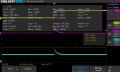
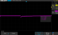
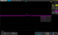
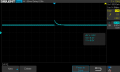
That is correct. This leads to three questions.It appears that channel 2 is riding on zero volts and channel 3 is riding on + 5 volts.
1) Why is this so?
2) What do we know about the shape and time duration of the spikes?
3) What are the voltages at the extreme tips of the rising spike and the falling spike for each of the two circuits?
After you have understood the significance of these answers there will be more questions to follow.