Will this power on / Efuse circuit work?

Thread Starter

robotDR

Joined Mar 17, 2020
138
Hello All,

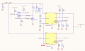
Thank you for taking a look. My intention for this circuit is to use the EFuse TPS259814 in parallel for inrush current limitation and also as an EFuse, and then I also wanted a battery disconnect with very low quiescent power.

As long as I have EN/UVLO low, it will be very little current draw from the EFuse.

So PWR_BTN is connected to an off board momentary button. When the user presses the button, the mcu gets powered up and holds MCU_PWR_EN high to keep power going to the system. The MCU also gets a feedback signal when a user presses the button hoping to turn it off, from PWR_BTN_FB.

My understanding of the cricuit is that Q3B starts open, and U13 EN/UVLO is pulled down through the resistor tree.

When a user presses the button, Q3B closes, U13 starts conducting VBATT_RAW to VBATT_RAW_FUSED. MCU powers up and holds MCU_PWR_EN high which closes Q3A and power stays on as long as MCU likes.

I want to maintain the UVLO and OVLO circuits and Q3B should only add about 400-500 mOhm to that drivng the gate to 0 and source at 3.4V-4.2V.

Please let me know what you think.

I expect U13 to pull about 25uA max with EN/UVLO pulled to gnd via the resistor tree. and ofcourse neither U13 or U16 to be conducting.
 

Attachments

I am not familiar with that TI IC, but I have a recent home project which uses a discrete current sensing latch as sort of an e-fuse. It uses a transistor Vbe as a current sense threshold voltage. Not very precise but good enough for what I was doing.

Mainly: I see you using a bunch of 0201 and 01005 chip resistors. If you know that you need chips that small, and you know that you can handle/assemble them, that is OK. But if you do not know that you can assemble those, then you probably cannot.

I am in general agreement with most of the other EEs I know: For my/our own use, I stay with 0603 and larger. I like to use a smallish 0805 pcb footprint for 0603 chips. My success rate in soldering an 0402 might be 50%. I have a very limited selection of 0402s in my lab and I use those only if absolutely necessary. I would not attempt anything smaller.
 

Thread Starter

robotDR

Joined Mar 17, 2020
138
Yeah these are going to be professionally assembled. If I have space left over I may increase to 0201.

I can rework 01005 fine enough but I don’t prefer it lol.
 

MisterBill2

Joined Jan 23, 2018
27,442
If you are limiting some "inrush current" by dropping the voltage, which is what I think I see, what effect will that voltage drop have on whatever process is being powered up?? And why are we not shown the Since we have no hint about the rest of the system that is a valid question. Why are we not shown the feed for the power button, even??
 
Hello All,

Thank you for taking a look. My intention for this circuit is to use the EFuse TPS259814 in parallel for inrush current limitation and also as an EFuse, and then I also wanted a battery disconnect with very low quiescent power.

As long as I have EN/UVLO low, it will be very little current draw from the EFuse.

So PWR_BTN is connected to an off board momentary button. When the user presses the button, the mcu gets powered up and holds MCU_PWR_EN high to keep power going to the system. The MCU also gets a feedback signal when a user presses the button hoping to turn it off, from PWR_BTN_FB.

My understanding of the cricuit is that Q3B starts open, and U13 EN/UVLO is pulled down through the resistor tree.

When a user presses the button, Q3B closes, U13 starts conducting VBATT_RAW to VBATT_RAW_FUSED. MCU powers up and holds MCU_PWR_EN high which closes Q3A and power stays on as long as MCU likes.

I want to maintain the UVLO and OVLO circuits and Q3B should only add about 400-500 mOhm to that drivng the gate to 0 and source at 3.4V-4.2V.

Please let me know what you think.

I expect U13 to pull about 25uA max with EN/UVLO pulled to gnd via the resistor tree. and ofcourse neither U13 or U16 to be conducting.
One other thing to understand:

I am an experienced design engineer, but I am completely unfamiliar with this TI IC. (Just to be clear, I generally like TI ICs; nothing against the company.) But if I were to design with such an unfamiliar IC, I would spend hours (not all at once) with the datasheet. Anytime we work with an unfamiliar IC there is a learning curve and also increased risk.

This IC is probably one which fewer engineers have designed with. So for me and for many other engineers to answer your question carefully will require hours. If you are lucky, you will find someone helpful who has used the IC. But if not, you might not find the sort of detailed help you are seeking.

When using an unfamiliar IC there is also the real risk of running into issues which are not mentioned in the datasheet. This happens more often than we would like.

Having said all that, a few years ago I DID design a novel power converter circuit using a TI chip which I had never used before. Significant risk there. But it worked out of the chute so to speak. As I say, I like TI ICs pretty well.
 

Thread Starter

robotDR

Joined Mar 17, 2020
138
If you are limiting some "inrush current" by dropping the voltage, which is what I think I see, what effect will that voltage drop have on whatever process is being powered up?? And why are we not shown the Since we have no hint about the rest of the system that is a valid question. Why are we not shown the feed for the power button, even??
The inrush isn’t limited by dropping voltage, but by slew rate control. Inrush current is from capacitance down stream.
 

MisterBill2

Joined Jan 23, 2018
27,442
" but by slew rate control " sounds a whole lot like dropping the voltage momentarily to reduce the current. But evidently that does not cause a problem.
And certainly, designing with a new device like this IC is going to present a learning experience. So I recommend building a prototype prior to production. Often the very first design needs a small adjustment, or maybe even two adjustments.. But you already knew that.
 
" but by slew rate control " sounds a whole lot like dropping the voltage momentarily to reduce the current. But evidently that does not cause a problem.
And certainly, designing with a new device like this IC is going to present a learning experience. So I recommend building a prototype prior to production. Often the very first design needs a small adjustment, or maybe even two adjustments.. But you already knew that.
I think that the idea is to limit inrush caused by C*dV/dt. Reduce dV/dt = slowing the voltage rise.
 

MisterBill2

Joined Jan 23, 2018
27,442
I think that the idea is to limit inrush caused by C*dV/dt. Reduce dV/dt = slowing the voltage rise.
Certainly that is how reducing inrush current works!.. Which amounts to lowering the voltage to limit the current. Not a constant voltage reduction, just a current-limiting reduction.
So my comment was probably not clear enough about the duration of the reduction being only momentary. sorry about the lack of clarity on that point.
 
Top