 Facebook
 Google
 GitHub
 Linkedin
I am inspecting a few PCB designs and seeing some unusual features and would love help identifying them.
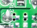
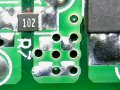
In two of the attached images, there appear to be unfilled holes that go all the way through the 2-layer PCB. The placement of the holes doesn't seem to align with locations for optional placement of components that just were not populated on the PCB.
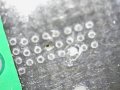
One image has a array of small metal "stamps" in a large metal area.
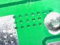
Final there is an array of small holes that appear to go through the top side coating layer, but not through the board. They even overlap the edge of a metal area. Strange.
If you have any ideas, I would love to hear them! Thanks.
In two of the attached images, there appear to be unfilled holes that go all the way through the 2-layer PCB. The placement of the holes doesn't seem to align with locations for optional placement of components that just were not populated on the PCB.
One image has a array of small metal "stamps" in a large metal area.
Final there is an array of small holes that appear to go through the top side coating layer, but not through the board. They even overlap the edge of a metal area. Strange.
If you have any ideas, I would love to hear them! Thanks.
Attachments
-
 505.3 KB Views: 8
 -
 507.3 KB Views: 8
 -
 376.8 KB Views: 8
 -
 433.3 KB Views: 8


