Facebook
 Google
 GitHub
 Linkedin
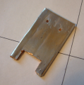
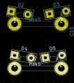
Couple things here: First, we're assuming they ARE heatsinks. We don't know that for sure. Second, we're assuming they run hot, hence, a need for heat sinking. If any of that is true then some of the issues raised are important. If not - then they are fairly moot points.
Component leads DO conduct heat to the boards they're soldered to. If that heat is high enough they can burn the board. I've seen power resistors mounted above the boards and over time the PCB becomes scorched from the radiant heat; primarily resistors. In fact, one technique of above board resistor mounting has been to create a 270˚ loop in the leads. This provides two functions; heat dissipation and shock/vibration protection. Thermal expansion and contraction is yet another benefit from such an arrangement. And this is not limited to resistors, though I've never seen it applied to anything else such as diodes. [edit] Now that I think of it I HAVE seen diodes with either a single or double loops. [end edit]

Component leads DO conduct heat to the boards they're soldered to. If that heat is high enough they can burn the board. I've seen power resistors mounted above the boards and over time the PCB becomes scorched from the radiant heat; primarily resistors. In fact, one technique of above board resistor mounting has been to create a 270˚ loop in the leads. This provides two functions; heat dissipation and shock/vibration protection. Thermal expansion and contraction is yet another benefit from such an arrangement. And this is not limited to resistors, though I've never seen it applied to anything else such as diodes. [edit] Now that I think of it I HAVE seen diodes with either a single or double loops. [end edit]
Last edited: