 Facebook
 Google
 GitHub
 Linkedin
I'm new to JFET's and I think 1 is out of whack in my Keithley197. So I'm looking at some lecture notes today, but I still don't know if this means the JFET is gone bad. I think it's a N-ch Vishay 2N4117A
http://pdf.datasheetcatalog.com/datasheet/vishay/70239.pdf
https://www.utwente.nl/en/tnw/slt/documentation/Equipment/GeneralEquipment/keithley197.pdf
An op-amp drives the gate low with -8.9823V, across a 1Meg to the gate, but it's at -7.4885V, so that's 1.5uA exiting the gate, isn't that huge?
Also the 330k drain resistor has the 2.00184V Vref on top, and the drain is at 1.88762V, so that's 346nA, if it's actually entering the FET. The Source is at around 10mV on the buffer/amp, and it varies a lot, 10s-100s iirc of mV on Voltage ranges) and it's not 60Hz or harmonics, or it has to be subtracted out, right now this junk signal is there, nearly 1:1 matching the bad readings, and throws stuff of, . But it's the rouge voltage on that JFET Source (but 3 others too), that I think is the problem.
I haven't tried to calculate any JFET eqn's yet, but isn't that bad ? And it's supposed to be a high Imp. JFET, so really high.
It's Q113 on page 66, and on page 50 you can see the 4 JFETs of the sampling multiplexer, Q113 is to sample the 2Vref, and the other 4 JFETs are for the range dividers.
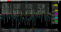
Here's Q113, w/ the Grn probe on Drain, blue on source, red on gate, yellow on gate drive, that was on 200V rng, in testmode with only the Q113 network running.
I'll have to check the othre JFets, what do u folks think ?
Ok in the last pic, it matches at any freq, as the gate voltage drops, the drain voltage increases, as the current into it from R111 drops. So indeed this JFET is a lot on-er than it should be.
I could have had current going into the shield pins, I guess there's some leakage and AC too, but I'm sure there's DC leakage/short problems
http://pdf.datasheetcatalog.com/datasheet/vishay/70239.pdf
https://www.utwente.nl/en/tnw/slt/documentation/Equipment/GeneralEquipment/keithley197.pdf
An op-amp drives the gate low with -8.9823V, across a 1Meg to the gate, but it's at -7.4885V, so that's 1.5uA exiting the gate, isn't that huge?
Also the 330k drain resistor has the 2.00184V Vref on top, and the drain is at 1.88762V, so that's 346nA, if it's actually entering the FET. The Source is at around 10mV on the buffer/amp, and it varies a lot, 10s-100s iirc of mV on Voltage ranges) and it's not 60Hz or harmonics, or it has to be subtracted out, right now this junk signal is there, nearly 1:1 matching the bad readings, and throws stuff of, . But it's the rouge voltage on that JFET Source (but 3 others too), that I think is the problem.
I haven't tried to calculate any JFET eqn's yet, but isn't that bad ? And it's supposed to be a high Imp. JFET, so really high.
It's Q113 on page 66, and on page 50 you can see the 4 JFETs of the sampling multiplexer, Q113 is to sample the 2Vref, and the other 4 JFETs are for the range dividers.
Here's Q113, w/ the Grn probe on Drain, blue on source, red on gate, yellow on gate drive, that was on 200V rng, in testmode with only the Q113 network running.
I'll have to check the othre JFets, what do u folks think ?
Ok in the last pic, it matches at any freq, as the gate voltage drops, the drain voltage increases, as the current into it from R111 drops. So indeed this JFET is a lot on-er than it should be.
I could have had current going into the shield pins, I guess there's some leakage and AC too, but I'm sure there's DC leakage/short problems
Attachments
-
 378.7 KB Views: 24
 -
 1.3 MB Views: 24
 -
 314.9 KB Views: 20
 -
 158.2 KB Views: 11
Last edited:


