What kind of band stop filter is this?

Thread Starter

ph_kloth

Joined Nov 9, 2020
3
Hi all,

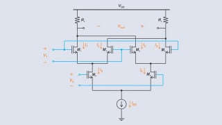
I have found this schematics generating a band stop filter design:

Schematics.png

The corresponding transmission is this here:

transmission.png

You see that this design generates a band stop at around 230Hz.

I have tried to find a similar topology in books and online but was not successful. Do you have any idea what this is? And if so, how to calculate the band stop frequency and width?

Thanks in advance for your help!

Philipp

P.S. I hope that I used the correct subforum. If not, please let me know!
 

LvW

Joined Jun 13, 2013
1,752
Are the shown simulation results derived from the shown circuit?
I am a bit surprised because of the low-frequency behaviour.
How can C11 and C12 transfer low frequency signals (down to DC)?
 

crutschow

Joined Mar 14, 2008
34,285
A filter with a narrow band reject is commonly called a notch filter.
In this case it consists of a low-pass and a high-pass filter in series.

You'd have to calculate the transfer function to determine its frequency response.
If you just want to change the notch frequency, then just change the value of the resistors and/or capacitors proportionally.
How can C11 and C12 transfer low frequency signals (down to DC)?
It doesn't go to DC, the low-frequency rolloff occurs below 0.1Hz (see below):

1604933470183.png
 

Thread Starter

ph_kloth

Joined Nov 9, 2020
3
A filter with a narrow band reject is commonly called a notch filter.
In this case it consists of a low-pass and a high-pass filter in series.

You'd have to calculate the transfer function to determine its frequency response.
If you just want to change the notch frequency, then just change the value of the resistors and/or capacitors proportionally.
Hey,

thank you for your response. But I don't think that it is simply a low pass and high pass in series. Ok I agree that the last op feedback part is only a low pass with a high gain and a very low cut off frequency (56Meg).

But the double feedback loop around the first OpAmp is somehow more complicated:

For example taking only one feedback loop of the first opamp like this:
Schematics_lead.png

you get at transmission which is very similar to the transmission of a lead compensator (https://ctms.engin.umich.edu/CTMS/index.php?aux=Extras_Leadlag).

transmission_lead.png

If you now add the second feedback loop, you get this:
Schematics_halfNotch.png

And for the transmission, this is not a highpass filter. It is something more. It is a lead compensator with something else. And this is what confuses me.

transmission_notch.png

For a highpass filter, the signal should go to -infinity for low frequencies. Here it stays at 0dB.

But good point, if you want to calculate sth like this, how would you start. I would like to implement this circuitry in Simulink and therefore calculate the transfer function T(s).

But I am not so well with calculating circuits.

Thanks for your help!
 
Top