Facebook
 Google
 GitHub
 Linkedin
I was wondering if someone could correct/add to the definitions I have written below. I'm trying to understand what the various specifications associated with N-Channel MOSFETs in the Mouser table mean so I can select one. I'll be switching the transistor on and off fairly slowly, feeding 12-14v into its gate, which will in turn trigger another 12-14v across the drain-source. The component drawing energy across the latter will draw in the neighborhood of 5 amps, so we're looking at around 60-70 watts. I want to get a MOSFET that won't even come close to overheating and I'm unclear about how to go about it. I've read a bit and wanted to see if forum members would be so kind as to confirm or correct my understanding of these key terms:
Id — Continuous Drain Current
This number indicates the limit for the current that can be passed across the Drain-Source circuit.
Vgs — Gate Source Voltage
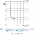
This number indicates the voltage differential that, when measured across the Gate and Source, results in the optimum operating condition, as indicated by the lowest resistance across the Drain-Source circuit. Applying voltage lower that Vgs results in a higher resistance on the Drain-Source circuit, and increased heat build-up in the MOSFET when power is passed through the Drain-Source circuit. Applying voltage higher than Vgs across the Gate and Source results in the same condition, and to a greater degree — that is, a volt higher than Vgs across the Gate and Source will generally increase the Drain-Source resistance (and heat) more than a volt lower will increase them. Systems should be designed to result in a voltage across the Gate and Source as close to Vgs as possible. It's better to be a little under than a bit over.
Vds — Drain Source Breakdown Voltage
This number indicates the voltage differential that, when measured across the Drain and Source, results in the resistance between these two being overcome and current being allowed to flow. This is a "fail mode" and as such, is above the limit for the voltage that should be switched with the component.
Rds On — Drain-Source Resistance
This number indicates the resistance measured across the Drain-Source circuit when the voltage differential between the Gate and Source is at Vgs.
Pd — Power Dissipation
This number indicates the limit of the MOSFET's ability to pass power across the Drain-Source circuit to a destination component without experiencing physical failure. Applying a particular voltage across the Gate and Source will result in a corresponding resistance across the Drain-Source circuit. Passing a given voltage through the Drain-Source circuit to a component with a particular resistance will result in a corresponding current passing across the Drain-Source circuit. This current can be calculated by dividing the voltage across the Drain-Source circuit by (the resistance across the Drain-Source circuit, added to the resistance across the component's leads). The power being dissipated can be found by multiplying this current by the voltage. This number must be kept under the Pd specification of the MOSFET.
I'm uncertain about all of these (*some especially), so please correct me. Thank you.
Id — Continuous Drain Current
This number indicates the limit for the current that can be passed across the Drain-Source circuit.
Vgs — Gate Source Voltage
This number indicates the voltage differential that, when measured across the Gate and Source, results in the optimum operating condition, as indicated by the lowest resistance across the Drain-Source circuit. Applying voltage lower that Vgs results in a higher resistance on the Drain-Source circuit, and increased heat build-up in the MOSFET when power is passed through the Drain-Source circuit. Applying voltage higher than Vgs across the Gate and Source results in the same condition, and to a greater degree — that is, a volt higher than Vgs across the Gate and Source will generally increase the Drain-Source resistance (and heat) more than a volt lower will increase them. Systems should be designed to result in a voltage across the Gate and Source as close to Vgs as possible. It's better to be a little under than a bit over.
Vds — Drain Source Breakdown Voltage
This number indicates the voltage differential that, when measured across the Drain and Source, results in the resistance between these two being overcome and current being allowed to flow. This is a "fail mode" and as such, is above the limit for the voltage that should be switched with the component.
Rds On — Drain-Source Resistance
This number indicates the resistance measured across the Drain-Source circuit when the voltage differential between the Gate and Source is at Vgs.
Pd — Power Dissipation
This number indicates the limit of the MOSFET's ability to pass power across the Drain-Source circuit to a destination component without experiencing physical failure. Applying a particular voltage across the Gate and Source will result in a corresponding resistance across the Drain-Source circuit. Passing a given voltage through the Drain-Source circuit to a component with a particular resistance will result in a corresponding current passing across the Drain-Source circuit. This current can be calculated by dividing the voltage across the Drain-Source circuit by (the resistance across the Drain-Source circuit, added to the resistance across the component's leads). The power being dissipated can be found by multiplying this current by the voltage. This number must be kept under the Pd specification of the MOSFET.
I'm uncertain about all of these (*some especially), so please correct me. Thank you.