 Facebook
 Google
 GitHub
 Linkedin
WFC Water Fuel Cell by Farlander
- Thread starter Farlander
- Start date
- Status
- Not open for further replies.
Scroll to continue with content
Indeed, how accurate is this program?Beware though SPICE might be lying.
What is this ringing? I notice it too coming from power supplies when directly connected to the cell... 18V 4.9 amp, 24V .83 amps, etc. they change pitch with changes in the water. I can hear the pitch change when I adjust frequency as well.You really don't want a zero resistance path to a MOSFET gate anyway, because it will "ring" at very high frequency
I appreciate your concern. I'll post before attempting anything drastic.This is not a good idea for you to try at this point. My concern is your safety.
I don't have much bucks, but I do have a 250 watt compaq desktop power supply.with an ATX form factor power supply, you can make a decent bench supply out of it for a few bucks
Tap water currently, ideally distilled, no electrolyte. The charging chokes and oxide coating on the electrodes are to prevent "electron leakage, allowing voltage to take over and perform the work" This has been a serious point of argument with traditional physicists. Here is an article suggested by a friend on the work voltage can perform http://hyperphysics.phy-astr.gsu.edu/hbase/electric/elewor.htmlK, wait a sec - are you using pure distilled water, tap water, or are you using an electrolyte solution?
It has it's limitations. For example, you can stress a component far beyond what "real world" limitations would be. In eblc1388's simulation with the 555, it's output is sourcing/sinking in excess of 450mA, which wouldn't work in the real world without letting the smoke out of the 555. You have to examine what the simulation is reporting, and correct situations like that where components would be subjected to excessive stresses; in this case the solution would be to increase the value of resistance between the output of the 555 timer and the gate to reduce peak current.Indeed, how accurate is this program?
Also, the simulation is reporting that the 555 output nearly reaches Vcc. This is definitely not real-world, as a bjt 555's output has a Darlington voltage follower. An output under load would peak at about Vcc-1.7v.
The ringing I'm talking about is at a very high frequency that you wouldn't be able to hear; in the 100kHz to 20MHz range.What is this ringing? I notice it too coming from power supplies when directly connected to the cell... 18V 4.9 amp, 24V .83 amps, etc. they change pitch with changes in the water. I can hear the pitch change when I adjust frequency as well.
The ringing you're hearing is most likely inductors vibrating due to the various currents flowing through them when you're alternatively placing them under no load/heavy load conditions.
Safety is paramount here. Fiddling around with high voltage near water is generally not conducive to good health for n00b's.I appreciate your concern. I'll post before attempting anything drastic.
")
If it's an ATX form factor supply, you can convert it pretty inexpensively.I don't have much bucks, but I do have a 250 watt compaq desktop power supply.
Arguably, the most expensive parts will be the banana jacks, depending on where you get them. Remember that banana jacks are generally rated for 10A, and the +5v and +3.3v can put out quite a bit more than that. You don't have to use banana jacks, though.
Since eblc1388 was kind enough to expand on the simulation, I figured I'd throw my hat in the ring, so to speak
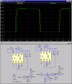
Here's an updated version of what both myself and eblc1388 have been tinkering with. The square wave generator has been replaced with two separate yet identical 555 circuits.
Values for R1 and R3 were selected to limit the 555's peak output current to 200mA. Note the upper plot, indicating current in R1 (green) and R3 (pink). R1 has +/-200mA current spikes both during the gate charge and discharge portions of the cycle, yet R3 has only a miniscule spike during discharge. This is because Q1 is carrying almost the entire load during discharge.
Note the lower plots. The red trace is the output from the first 555 timer; you can see that loading does have an effect on the output - otherwise it would appear as a nearly perfect rectangular waveform.
The voltage on the gate of M1 (green) charges up slightly faster than the gate of M2 (pink). This is because I didn't bother to compensate for the addition of D1 (1N5817 Shottky 1A diode) when selecting the value of R3. D1's Vf accounts for the difference in peak voltage between the two gates (about 0.3v)
The really striking difference between the modified original driver circuit (changing R1/R2 values) and the proposed modification is the gate discharge cycle. The gate of M2 (pink) drops from about 8v to 2v in about 0.33uS; it takes the gate of M1 over three times that long to make the same transition. This means that M1 will be heating up quite a bit more than M2.
Additionally, since the discharge current of M2's 555 has been virtually eliminated, we might elect to use a somewhat lower value for R3, since the average power dissipation has already been cut in half.
Attachments
-
 63.9 KB Views: 31
 -
4.1 KB Views: 18
Already did that before I saw your post. The result is about the same:OK, but now you're loading the single 555's output by both gate circuits.
Clone your 555 circuit, and re-label the nets 555out1 and 555out2.
I finally find out why your circuit appears slower. It is slower because the total gate series resistance is larger. If I increase my series resistance to match yours, then the rise time become the same. Now the fall time of mine suffer and your PNP discharge scheme wins hand down.
Attachments
-
 19.7 KB Views: 93
 -
 20.6 KB Views: 91
OK, you're looking at the current through the load resistors, not the current through the gate resistors.
[eta]
Silly me, I didn't see your comment between your two plots. Yes, you have to make things equal.
Comparing currents between R1 and R3 will tell you quite a bit.
I overlooked the values that you used for R8 and R10 on the 555 timers.
Increase R8/R10 to 1.5k. That will keep the discharge current (555 pin 7) to a safe value. They're only rated for 15mA; and your 470 Ohms causes 30mA current during discharge.
Change R7/R9 to 6.8k to keep approximately the same frequency range.
(edited to correct reference designators)
Last edited:
I was joking when I said SPICE was lying. I picked that up from what Bob Pease have always said and I agree with him.Indeed, how accurate is this program?
SPICE is not lying. It is doing its best to simulate the circuit condition using model of the circuit elements. As with all models, one cannot have a 100% accurate model which express the complete behavior of a part under all circumstances, including overload conditions, thus the result of SPICE calculation from all these models should be view with care.
Good day
I tested the oscillator with different R values at R7/R8. These are the results.
http://thewaterfuelsite.com/page2.htm
I tested the oscillator with different R values at R7/R8. These are the results.
http://thewaterfuelsite.com/page2.htm
Your waveforms ('scope photos) are meaningless unless you document where in the circuit you took them from.
[eta]
If the square waves with the trailing 'ramps' were taken from your MOSFET's gate, you have problems that my proposal will fix.
You need 10:1 probes.
[eta]
If the square waves with the trailing 'ramps' were taken from your MOSFET's gate, you have problems that my proposal will fix.
You need 10:1 probes.
Last edited:
Ok I fixed the circuit... I am actually getting gated square wave pulse trains now YAY! Thanks
I'm going to begin work on the MOSFET driver, but first, to convert the ATX supply to a bench top power source.
To build the power supply I apparently need a 10ohm, >10W resistor to connect the +5v (red) and 0v (black) output wires together (not sure why)
Then, the green (power ON) connects to black (0v) via a switch.
As for the MOSFET driver circuit, I don't have the 1N5817 Diode or the 2n2907 transistor, and I need some binding posts for the power supply. Should I be able to find these at radioshack or am I placing another order with jameco?
HOOWAH
What was the incorrect configuration, and what did you do to fix it?Ok I fixed the circuit... I am actually getting gated square wave pulse trains now YAY! Thanks
The ATX supplies are switchers. They won't regulate properly unless they have a load on the +5v supply. If you're desperate/in a hurry, Radio Shack sells a pair of 10 Ohm, 10W power resistors in a bubble pack for around $2. If a store is close by, it may actually be cheaper to buy them there than ordering them online and paying shipping charges.I'm going to begin work on the MOSFET driver, but first, to convert the ATX supply to a bench top power source.
To build the power supply I apparently need a 10ohm, >10W resistor to connect the +5v (red) and 0v (black) output wires together (not sure why)
I used a miniature SPDT switch on mine. A black wire goes to the common terminal (center), the green power ON lead goes to the lower terminal, and I have a yellow LED connected to the upper terminal of the switch via a 330 Ohm resistor to the violet (purple) standby +5V that tells me the supply has line power connected. When the supply is turned ON, the standby light goes out; but I have a couple of green LEDs on +3.3v and +5v to indicate that the voltages have come up. There was no point in unnecessarily loading the +12v, -12v and -5v supplies with an LED or complicating the assembly.Then, the green (power ON) connects to black (0v) via a switch.
Oddly enough, RadioShack might be the least expensive place to get binding posts. Keep in mind, the Radio Shack binding posts are rated for a maximum of 10A, and your +5V supply can likely output more than twice that. I doubled up on my +5v and +3.3v posts; each has a matching ground post.As for the MOSFET driver circuit, I don't have the 1N5817 Diode or the 2N2907 transistor, and I need some binding posts for the power supply. Should I be able to find these at radioshack or am I placing another order with Jameco?
They sell a pack of four (two red, two black) for about $4. The problem is, they're very cheaply made, and the nickel-plated lugs that come with the binding posts are a PITA to solder wires to. If you haven't cleaned them with isopropyl alcohol, are using a good hot soldering iron and flux with clean solder, you won't get a good solder joint.
2N2907 and it's plastic-encapulated equivalent PN2907's are also available at RS. However, you might consider buying 10 at a time from Jameco, Digikey or Mouser as well as a supply of 2N2222's (basically complementary transistors) which will be useful in future projects.
The 1N5817 Shottky diodes are getting to be a bit tricky to find (that means expensive.) Radio Shack does not carry them. Jameco, Digikey and Mouser do carry them. For this application, you could also use 1N5818 or 1N5819 diodes; the 1N5817 diodes have a PIV of 20, the 1N5818 have a PIV of 30, 5819, 40v. With Shottky diodes, the higher the PIV, the higher the Vf (forward voltage). For your application, the lowest Vf is desireable.
The idea of using these 1A Shottky diodes is that it allows for a very fast charge of the MOSFET's gate, with a very low Vf, and also they turn off VERY quickly. You might think you could use a 1N4000 series, but those are extremely slow by comparison to switch on and off, and have three times the Vf.
1N914/1N4148 diodes would be nearly as fast as the Shottky diodes specified, but could only carry 1/10 the current, and would also have 3x the Vf.
Schottky diodes are getting much harder to find due to the industry gravitation to dedicated driver ICs, synchronous rectifiers, and other developments. Industry is driven to reduce parts count; as that decreases inventory, assembly costs and increases reliability. Unfortunately lately it also makes it tough on the hobbyist - unless you're a good "scrounger".
The MOSFETs that you've salvaged are reasonably good for your application, but they do have an Achilles' heel, and that is their relatively large gate charge requirement.
In very broad terms, MOSFETs that are capable of carrying high current (Id rating) typically have a high gate charge requirement. That's because in order to carry the high currents, the internal physical junctions must be correspondingly larger to handle the electron/hole flow; which results in a larger area to be charged/discharged.
MOSFET manufacturers are making great strides in increasing current handling capabilities while decreasing drive requirements.
It was a careless mistake, I forgot to hook up pin#1 to ground on the second oscillator, so it was completely disabled. Now the circuit works great! I was curious though, could you explain how the capacitor values at pin5 and at pin6/2 affect the output?What was the incorrect configuration, and what did you do to fix it?
Are these the same as zener diodes? Why is a lower Vf better?The idea of using these 1A Shottky diodes is that it allows for a very fast charge of the MOSFET's gate, with a very low Vf, and also they turn off VERY quickly. You might think you could use a 1N4000 series, but those are extremely slow by comparison to switch on and off, and have three times the Vf.
Good that you found it. Little things like that can drive one bonkers.It was a careless mistake, I forgot to hook up pin#1 to ground on the second oscillator, so it was completely disabled. Now the circuit works great!
The 10nF cap from pin 5 to ground helps to keep the Control Voltage stable. Without a cap there, the frequency output will be less stable, particularly if there is noise on Vcc. Look in National Semiconductor's datasheet for the LM555 at the internal schematic on page 1, and you'll see that pin 5 is connected to the upper limit (2/3 VCC) of the threshold voltage divider circuit (three 5k resistors in series from Vcc to GND).I was curious though, could you explain how the capacitor values at pin5 and at pin6/2 affect the output?
No, Schottky diodes are not the same as Zener diodes.Are these the same as zener diodes? Why is a lower Vf better?
Zener diodes are simple shunt voltage regulators.
As far as "Why is a lower Vf better?", the rise time of the gate is improved, along with the power dissipation in the diode will be significantly less.
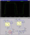
See the attached simulation. The two circuits are identical, except for the diodes used. The display has been zoomed in to only show the gate charge portion of the cycle.
On the left, a 1N4148 switching diode is pressed to the limits of it's ratings (green trace). On the right, the 1N5817 Shottky diode has a lower Vf, so the gate charge is building up more quickly (pink trace).
The red trace is the current flow through R1, there is a 220mA peak at time 7.8uS. The "flat spot" you see on the gate voltages between 7.9uS and 8.1uS is the "Miller charge"
I would've used a 1N4000 series to show how slow they are, but none exist in the default library.
Attachments
-
 65.9 KB Views: 47
Going back to your webpage, you mention that C1/C2 are 1pF. There are no reference designators on your schematic, so there is no way to figure out what two caps are actually 1pF. Additionally, since 1pF capacitors are so small in value, they would have no measurable effect on your circuit. Did you mean 1nF instead?
Just to keep things straight:
1nF = 1000pF
1uF = 1000nF
1mF = 1000uF
1F = 1000mF
[eta]
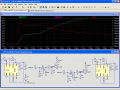
Looks like you are running the left half of your circuit at VERY high frequencies (up to nearly 1MHz). The left side is supposed to be the enable/disable circuit for the right side. This portion should be kept at a relatively low PRF, no where near as high as the right side.
You need to figure out why it's taking so long for the signal to drop from Vcc to GND (traces on the right side).
I suggest that you don't try to run the MOSFET gate driver at more than around 50kHz, or you may start burning out MOSFETs due to the porportionately greater amount of time spent in the linear (high resistance) region.
Just to keep things straight:
1nF = 1000pF
1uF = 1000nF
1mF = 1000uF
1F = 1000mF
[eta]
Looks like you are running the left half of your circuit at VERY high frequencies (up to nearly 1MHz). The left side is supposed to be the enable/disable circuit for the right side. This portion should be kept at a relatively low PRF, no where near as high as the right side.
You need to figure out why it's taking so long for the signal to drop from Vcc to GND (traces on the right side).
I suggest that you don't try to run the MOSFET gate driver at more than around 50kHz, or you may start burning out MOSFETs due to the porportionately greater amount of time spent in the linear (high resistance) region.
Last edited:
The website is still in progress, I've been making frequent changes but it's a lot of work to update. I'm hoping once I update it a few times the process gets easier and I can use it as a journal and reference tool. I will also be redrawing the circuit with component labels and the new values -- currently I have R7/R9 at 470 ohms, R8/R10 at 1.5k ohms, do you recommend 1.5k and 6.8k as your latest schematic shows?
The scope shots you see are actually inverted. I had the negative probe hooked to the 555 output. They are simply to show the max and min frequency of one 555 chip given different R values.
I'm having a hard time understanding capacitor values. I bought a random assorted collection from RS and organized them into a nice little box with dividers. The numbers of the ceramic disc caps I have are
1
7
10
15
68
101
151
221
561
From what I've read, 1 = 1 pF, 10 = 10 pF, 101 = 100 pF, 221 = 220 pF, etc. Maybe I'm way off...
Thanks kindly
I understand. But, the more you update it, the easier it will be - because you will become more proficient, and by updating it more often, you'll have fewer changes to make.The website is still in progress, I've been making frequent changes but it's a lot of work to update. I'm hoping once I update it a few times the process gets easier and I can use it as a journal and reference tool. I will also be redrawing the circuit with component labels and the new values
Ahh, do you mean eblc1388's latest schematic?-- currently I have R7/R9 at 470 ohms, R8/R10 at 1.5k ohms, do you recommend 1.5k and 6.8k as your latest schematic shows?
I see. It's really best to show waveforms referenced to ground, unless it's special circumstances like the Vgs of a P-channel MOSFET; in that case your reference point would be the source terminal of the MOSFET.The scope shots you see are actually inverted. I had the negative probe hooked to the 555 output. They are simply to show the max and min frequency of one 555 chip given different R values.
You're correct in how you're reading the ceramic cap values.I'm having a hard time understanding capacitor values. I bought a random assorted collection from RS and organized them into a nice little box with dividers. The numbers of the ceramic disc caps I have are
1
7
10
15
68
101
151
221
561
From what I've read, 1 = 1 pF, 10 = 10 pF, 101 = 100 pF, 221 = 220 pF, etc. Maybe I'm way off...
Keep in mind though, 220pF = 0.22nF = 0.00022uF.
If you placed ten 220pF caps in parallel, you'd have 2.2nF.
The RS ceramic disc capacitor assortment isn't as good as it used to be; you wind up with lots of caps from 1pF to 10pF and not many of the larger values. The small values really aren't very useful unless you're working on circuits designed to run in multiple MHz and higher RF ranges. On the plus side, the values marked are in a much more consistent format than they used to be, and the tolerances are actually much better.
see
http://forum.allaboutcircuits.com/showthread.php?t=17703
I detailed the ATX power supply conversion in the above thread. After testing, I've found that the grey 'sensor' wire does not need to be hooked up to anything for the unit to function. Reports I read said it should be paired with an orange (3.3v). When I do this, no apparent change in function...
The sensor wire itself outputs about .2v
Hey people
Description MFG # Jameco # Qty Ordered Ship Date Qty To Ship Balance To Ship Price Ea USD Total
@ DIODE SCHOTTKY,1N5818,1.0A
30V VARIOUS 1N5818 177957 1/09/09 10
$0.07 $0.70 REMOVE @DIODE SCHOTTKY,1N5817,1.0A
20V (10) VARIOUS 1N5817 177949 1/09/09 10
$0.12 $1.20 REMOVE @ DIODE SCHOTTKY,1N5819,1.0A
40V VARIOUS 1N5819 177965 1/09/09 10
$0.10 $1.00 REMOVE REFILL PKG,CAPS,CERAMIC
(520 PCS.) VARIOUS 00130232 130232 1/09/09 1
$23.45 $23.45 REMOVE PNP GEN.PURPOSE
ST MICRO 2N2907 924297 1/13/09 5
$0.46 $2.30 REMOVE NPN GEN.PURPOSE
ST MICRO 2N2222 924289 1/09/09 5
$0.55 $2.75 REMOVE POT,10K,RV24AF-10-20K-B10K,
LINEAR,KNURLED,1/2 WATT,.531 ALPHA ELECTRONICS(TAIWAN) RV24AF-10-20K-B14 264411 1/09/09 5
$1.39 $6.95 REMOVE POT,5M,RV24AF-10-40R1-B5M,
LINEAR TAPER,1/2 WATT,1.32 ALPHA ELECTRONICS(TAIWAN) RV24AF-10-40R1-B56 255733 1/09/09 2
$1.65 $3.30 REMOVE IC,LM555CN, DIP-8,
TIMER SINGLE 0-70DEG C VARIOUS LM555CN-R 27423 1/09/09 6
Is there a particular mosfet you would recommend, with low ON resistance, low gate charge requirement, and high voltage/current capacity? Prefer around 120V / 10amp rating. I'll be ordering very soon!
Ok, next problem.
I want to apply high volts to the submerged electrodes. Can I use the auto ignition coil in series with the secondary winding of an isolated 110V/220V step up transformer? I'm not so much concerned about wave form at this point just getting high volts and phase separation.
Muchisimas gracias
p.s. why doesn't my profile pic work?
I was just getting ready to order some stuff from jameco.The MOSFETs that you've salvaged [IRF3710] are reasonably good for your application, but they do have an Achilles' heel, and that is their relatively large gate charge requirement.
Description MFG # Jameco # Qty Ordered Ship Date Qty To Ship Balance To Ship Price Ea USD Total
@ DIODE SCHOTTKY,1N5818,1.0A
30V VARIOUS 1N5818 177957 1/09/09 10
$0.07 $0.70 REMOVE @DIODE SCHOTTKY,1N5817,1.0A
20V (10) VARIOUS 1N5817 177949 1/09/09 10
$0.12 $1.20 REMOVE @ DIODE SCHOTTKY,1N5819,1.0A
40V VARIOUS 1N5819 177965 1/09/09 10
$0.10 $1.00 REMOVE REFILL PKG,CAPS,CERAMIC
(520 PCS.) VARIOUS 00130232 130232 1/09/09 1
$23.45 $23.45 REMOVE PNP GEN.PURPOSE
ST MICRO 2N2907 924297 1/13/09 5
$0.46 $2.30 REMOVE NPN GEN.PURPOSE
ST MICRO 2N2222 924289 1/09/09 5
$0.55 $2.75 REMOVE POT,10K,RV24AF-10-20K-B10K,
LINEAR,KNURLED,1/2 WATT,.531 ALPHA ELECTRONICS(TAIWAN) RV24AF-10-20K-B14 264411 1/09/09 5
$1.39 $6.95 REMOVE POT,5M,RV24AF-10-40R1-B5M,
LINEAR TAPER,1/2 WATT,1.32 ALPHA ELECTRONICS(TAIWAN) RV24AF-10-40R1-B56 255733 1/09/09 2
$1.65 $3.30 REMOVE IC,LM555CN, DIP-8,
TIMER SINGLE 0-70DEG C VARIOUS LM555CN-R 27423 1/09/09 6
Is there a particular mosfet you would recommend, with low ON resistance, low gate charge requirement, and high voltage/current capacity? Prefer around 120V / 10amp rating. I'll be ordering very soon!
Ok, next problem.
I want to apply high volts to the submerged electrodes. Can I use the auto ignition coil in series with the secondary winding of an isolated 110V/220V step up transformer? I'm not so much concerned about wave form at this point just getting high volts and phase separation.
Muchisimas gracias
p.s. why doesn't my profile pic work?
Why don't you look in LTSpice?Is there a particular mosfet you would recommend, with low ON resistance, low gate charge requirement, and high voltage/current capacity? Prefer around 120V / 10amp rating. I'll be ordering very soon!
Start a new schematic, plop in an "nmos" part, then right-click on it, and then "Pick new MOSFET".
You can then sort by any column heading by clicking on it.
Try sorting by GateChg(nC). You want a low gate charge, and low Rds(on), with a voltage level you can live with.
No. 110V/220V transformers were designed to run on a 60Hz sinewave, where auto ignition coils are "broadband".Ok, next problem.
I want to apply high volts to the submerged electrodes. Can I use the auto ignition coil in series with the secondary winding of an isolated 110V/220V step up transformer?
Besides, if you used a GM HEI coil driven by 12v, you'd probably be getting in the vicinity of 100kv. You will have to use pure distilled water; any impurities will create a conduction path. You should probably start off running the coil from the 3.3v or 5v supply.
60kv will jump a dry air gap of 20mm (just over 3/4") at sea level; basically 3kv/mm
Check out this WIKI article on dielectric strength:
http://en.wikipedia.org/wiki/Dielectric_strength
Last edited:
- Status
- Not open for further replies.


