voltage dependency for PWM generator frequency

Thread Starter

pumpkinpie

Joined Aug 7, 2024
37
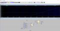
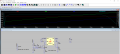
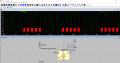
Hi. I have a PWM signal generator IC LTC6992-1 in my circuit, frequency of which is needed to be controlled by the DC source feeding the whole circuitry. In the schematic file the MOD input is set to be 0.5V to hinder confusion while commenting on frequency, normally it is desired to be dictated by the source as well. The 6990 model allows frequency control with voltage but with a constant %50 duty cycle fot the output. I need to control both so I also appreciate any solution that merges the two models somehow (Its even better considering the 6990 has an enable pin). Normally the frequency of the device is set by the three resistors R1 R2 and Rset. Frequency adjustment relies on the changes in Rset value so I came up with few ideas like using a potentiometer in series but that requires mechanical action rather than an internal voltage referencing. Using digital pots requires some controller circuitry so I had to give up on that too. Also, I dont have enough familiarity with FETs as well and I felt like operating them on the linear region precisely would demand lots of math on current and power limitations. As I got no other ideas on implying a continuous relation between the busbar voltage and the variable resistance I decided to set some modes and determine tresholds for each like first MOSFET is to be switched on when 40V is reached and it goes on with increments of 10 Volts for the other switches. To do so I thought of placing zeners between the gates of the MOSFETs and nodes with divided voltages but since they also allow voltages below 10 volts the switching tresholds are not as desired. How can I create this dependency in an analog or somewhat digital manner without using a considerable number of comparators and sources?

file updated*
 

Attachments

Last edited:

crutschow

Joined Mar 14, 2008
38,316
Below is the sim of your circuit using an LM339 quad comparator IC to select the frequency resistors:
The comparator output is an open-collector BJT that connects to ground when the (-) input is higher than the (+) input.
I've attached the files for the LM339 comparator.

1723152240678.png
 

Attachments

Last edited:

Thread Starter

pumpkinpie

Joined Aug 7, 2024
37
Below is the sim of your circuit using an LM339 quad comparator IC to select the frequency resistors:
The comparator output is an open-collector BJT that connects to ground when the (-) input is higher than the (+) input.
I've attached the files for the LM339 comparator.

View attachment 328826
Great. I thought of using comparators but had given up on them since they bring about the need for more power sources. But theres no simple alternative for those ig. I dont know why there is not an observable starting time in the simulation results you provided. And these Va,b,c,d outputs looks more clean compared to those my simulation gave me. Each one of them is distorted in a similar manner at 7.2 7.4 7.6 ms. Might that happen because of wrong use of comparators? I dont think theres anything wrong but I see no difference other than the labels for comparators so I may be missing sth about the use of the comparator as a quad comp rather than 4 separate ones. I would also love to hear about your opinion on controlling the frequency through voltage in a continuous manner rather than setting discrete modes.
 

Attachments

crutschow

Joined Mar 14, 2008
38,316
why there is not an observable starting time in the simulation results you provided.
Don't understand your question.
The starting time is at 0 seconds on the plot.
--on controlling the frequency through voltage in a continuous manner rather than setting discrete modes.
Below is the sim of the circuit with an op amp voltage-to-current circuit that sinks 0-20µA from the SET control pin to ground, to control the output frequency for a 0-1V input.
The negative feedback from R3 means that the voltage across it equals the input voltage, thus the SET current through the transistor equals V(source) / R3.
If you want the input to be a higher full-scale voltage, you can just add a 2-resistor attenuator at the op amp (+) input.

The sim shows a frequency adjust range of about 17KHz to 228kHz for the DIV value shown.

(The TLV915x (x = 1, 2, 4) in the simulation is a low-cost, rail-rail op amp with good offset, slew-rate, and frequency response specs, that can operate with a 3V supply.)

1723169514440.png
 

Attachments

Last edited:

Thread Starter

pumpkinpie

Joined Aug 7, 2024
37
Don't understand your question.
The starting time is at 0 seconds on the plot.
Below is the sim of the circuit with an op amp voltage-to-current circuit that sinks 0-20µA from the SET control pin to ground, to control the output frequency for a 0-1V input.
The negative feedback from R3 means that the voltage across it equals the input voltage, thus the SET current through the transistor equals V(source) / R3.
If you want the input to be a higher full-scale voltage, you can just add a 2-resistor attenuator at the op amp (+) input.

The sim shows a frequency adjust range of about 17KHz to 228kHz for the DIV value shown.

(The TLV915x (x = 1, 2, 4) in the simulation is a low-cost, rail-rail op amp with good offset, slew-rate, and frequency response specs, that can operate with a 3V supply.)

View attachment 328869
This looks really good. It will be the first time I use an opamp in such functionality and it looks like a fine solution here. For the voltage range I will use a simple voltage divider to get 0-100V. By the way, I meant the time it takes for the LTC6992 to start generating output by starting time. I get the output waveform after something like 6.19ms, for the circuit in post #2. I will post all the alternatives I created once finalized and hope you can give me some input on what are the weak points. Thank you.
 

crutschow

Joined Mar 14, 2008
38,316
the time it takes for the LTC6992 to start generating output by starting time. I get the output waveform after something like 6.19ms, for the circuit in post #2.
Okay.
That may be an artifact of the IC model, or it may actually represent the time it would take for the real circuit to start generating an output after the power is applied.
Won't know which, until you build an actual circuit (if that time is important in your application).
 

Thread Starter

pumpkinpie

Joined Aug 7, 2024
37
Okay.
That may be an artifact of the IC model, or it may actually represent the time it would take for the real circuit to start generating an output after the power is applied.
Won't know which, until you build an actual circuit (if that time is important in your application).
https://beta-tools.analog.com/timerblox/LTC6992 Looking at this tool I think it normally takes some time to start operating. I also wonder why there is an uic command even though there is no specified initial conditions for any nodes? When I remove the "uic" the simulation window does not even open. Does the command allow us to simulate quickly by disregarding the steady state calculations and assuming 0V at any nodes? I thought you added the 7m time to start saving data(as well as the source delay) to account for that 6.19m delay but considering your answer it must have another purpose right? when removed, there is a weird spike in the Vset at the very beginning of the simulation that lasts a few tens of nanometers. Lastly and most importantly, I think this current control is executed in the BJT's active region where it amplifies the base current by β, 300 for the part used in this circuit. In the simulation, Vb>Ve all the time, which is expected for the transistor to work but Vb exceeds the Vc after some time. Doesnt it imply saturation since both junctions are forward biased now? It seems like it doesnt have any particular effect as the Ic/Ib ratio remains the same and frequency keeps increasing even after Vb becomes larger than Vc(=Vset). Is that because the builtin voltage difference between the base emitter junction is more than how much Vb exceeds the Vc in this simulation? Shouldnt the turquoise curve start decreasing right after the intersection of red and green curves?
 

Attachments

crutschow

Joined Mar 14, 2008
38,316
I also wonder why there is an uic command
Sometimes the sim will get hung up when doing the normal bias calculation at the start, so I use the uic command, which then starts the transient analysis with all nodes being zero.
It has no effect on the sim results after that.
I thought you added the 7m time to start saving data(as well as the source delay) to account for that 6.19m delay
Yes, that was just to avoid displaying the first 6.19ms of no signal output.
but Vb exceeds the Vc after some time. Doesnt it imply saturation since both junctions are forward biased now?
Yes.
But Vb has to exceeds Vc by about 0.6V (Vb = 1.6V here) before the transistor saturates.
If you look at Vce, you will see that the transistor saturates (Vce near 0V) when the op amp (+) input reaches 1V.
 
Last edited:

Thread Starter

pumpkinpie

Joined Aug 7, 2024
37
Sometimes the sim will get hung up when doing the normal bias calculation at the start, so I use the uic command, which then starts the transient analysis with all nodes being zero.
It has no effect on the sim results after that.
Yes, that was just to avoid displaying the first 6.19ms of no signal output.
Yes.
But Vb has to exceeds Vc by about 0.6V (Vb = 1.6V here) before the transistor saturates.
If you look at Vce, you will see that the transistor saturates (Vce near 0V) when the op amp (+) input reaches 1V.
does the opamp align its output through the negative feedback during the process? When the Vb drops below a certain value that cause the Ve to decrease and then since it is a negative feedback path, the output voltage of the opamp, Vb is increased and kept higher than Ve and vice versa. this way it keeps a certain (0.55V) difference between the base and emitter. I got that transition from the linear region to saturation occurs only when Vb exceeds Vc by a certain amount, however in this case it seemed a bit larger than ususal to me, is 0.6V ok? and the Vce goes as near as 5mV to zero which again is a surprise to me since the typical values are a few hundreds of milivolts I guess? I think it highly depends on the BJT used but since I havent encountered such values I wanted to clarify. Please let me know if there are any other limitations other than the maximum and minimum current set by the 6992 and calculation of the maximum and minimum input voltage allowed for opamp through Imax.Rset=Vmax Imin.Rset=Vmin.
 

Thread Starter

pumpkinpie

Joined Aug 7, 2024
37
I also want to add some enabling network into each alternative and for the one with multiple modes I need AND(better if its 3 or 4 input but 2 is ok too) OR and INV gates that can work with 3.3 or 5V. I decided to use 74HC(04 08 32) series for all but I would like to hear from you if you have any other suggestions. The above format for enabling depends on adjusting the input to the gate driver. If a direct enabling such as turning the driver off when the general enable input is low and on when its high is needed, are there any options other than conditioning the supply voltage of the driver? Being aware of the fact that it is highly discouraged and inefficient to interfere with the supply of the component, just as in the image, is it the best to achieve this level of enabling at the input net of the driver as well? By the way thank you so much for your effort and time for all my posts and replies.
 

Attachments

Last edited:

crutschow

Joined Mar 14, 2008
38,316
does the opamp align its output through the negative feedback during the process? When the Vb drops below a certain value that cause the Ve to decrease and then since it is a negative feedback path, the output voltage of the opamp, Vb is increased and kept higher than Ve and vice versa. this way it keeps a certain (0.55V) difference between the base and emitter.
Yes, that's the magic of negative feedback.
transition from the linear region to saturation occurs only when Vb exceeds Vc by a certain amount, however in this case it seemed a bit larger than ususal to me, is 0.6V ok?
Yes.
Why do you think a lower value is "usual".
That's the typical forward drop of a diode, in this case the the base-collector diode junction.
the Vce goes as near as 5mV to zero which again is a surprise to me since the typical values are a few hundreds of milivolts I guess?
The Vce is somewhat proportional to the collector-emitter current.
But in this case, current starts flowing through the base-collector junction (look at the transistor base current), thus causing Vce to go near zero.
 

Thread Starter

pumpkinpie

Joined Aug 7, 2024
37
Do you just want to disable the output, or do you need to power down the circuit?
If possible, I want to power down. here is one of the examples with enable. this may better illustrate what I have been trying to do. In this configuration I simply disable the gate driver when the source voltage is below the treshold for PWM generation or when enable is low. One positive side of doing it this way is that there is no floating input. The MOSFET Vds is not enough for this application because source voltage increases to 100V(not likely to do so in reality i guess but still) but I used it to model V(N002) properly. The other MOSFETs with high gate charges and capacitance exhibit slower operation and therefore more right-tringular-like waveforms amplitudes of which cant even get to the source voltage level when the MOSFET is not conducting. I wonder why the fall time of the V(N002) is usually really low but the rise time is changing significantly with MOSFET selection. Might that stem from the existence of that 1mH inductor there, somehow making it harder to pull the voltage up than going down to ground level? It is a bit exaggerated to model the inductive effects of the wiring and the resistance. Inputs to 6992 and 6990 is fixed to make observations easier.
 

Attachments

Thread Starter

pumpkinpie

Joined Aug 7, 2024
37
So when, exactly, you you want to power down and when to power up?
What is the signal for this power up and down?
A voltage input that allows us to power up or down whenever we want. when this input is high and the circuit is operating, the driver is fed with PWM when the treshold is exceeded, when low, the whole circuitry doesnt operate.

How much power can this circuit consume?
This circuit is a chopper aiming at dissipating the excess energy through the resistor when the busbar exceeds the treshold. The maximum power dissipation is not specified and I honestly dont know what are the limiting parameters.
 

crutschow

Joined Mar 14, 2008
38,316
A voltage input that allows us to power up or down whenever we want. when this input is high and the circuit is operating, the driver is fed with PWM when the treshold is exceeded, when low, the whole circuitry doesnt operate.
By "exactly" I meant what is the "threshold" high voltage value and what is the low voltage value.
I can't do a design for "high" and "low".

I meant what is the allowed power consumption of this added control circuit.
Is it critical?
 

Thread Starter

pumpkinpie

Joined Aug 7, 2024
37
By "exactly" I meant what is the "threshold" high voltage value and what is the low voltage value.
I can't do a design for "high" and "low".

I meant what is the allowed power consumption of this added control circuit.
Is it critical?
sorry for the misunderstanding. The high and low tresholds are not specified either. I assume 3.3V for high min. and 1V for low max. will be ok though. about the power limitations, since this whole enabling thing is a vague design demand, I have to make assumptions here as well and say it is fine as long as it consumes less power than the functional circuitry.
 

crutschow

Joined Mar 14, 2008
38,316
Is this what you want?
Any of the ENx inputs logic high will apply power to the circuit.
M1 must be a logic-level P-MOSFET (Max Vgs(th) of 1.5V).

1723494551479.png
 
Top