Using MOSFET/JFET as a switch

Thread Starter

makaron

Joined Dec 17, 2011
18
Hello everyone,

I designed and built a circuit but made some mistakes during the design process and now would like to get some help before trying to fix them.

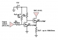
Basically I have a MCU which outputs a specified voltage with a DAC. After the DAC I wanted to have a way to switch where the output voltage goes to. Because relays are big and bulky, cost much etc, I decided to make a switch using MOSFETs. I found a schematic on the internet and designed my schematic based on it.


(I have many of these in parallel for switching.)
ADC shows where my DAC (yes, I accidentally drew ADC on the schematic) output voltage goes to. FET is P channel depletion MOSFET.
Now I see that there are 2 problems with this schematic:
1) If my DAC output voltage is low, then resistor bridge formed with 10k resistor and NPN transistor does not function
2) P channel depletion MOSFET is almost impossible to find (I was a genius an used enchancement MOSFET..)

Now I have to idea to make following changes to my schematic:


Instead of MOSFET I am thinking on using a JFET. (Have not added the bleed resistor on the schematic.)
I would need to have as small voltage drop on the FET as possible (milliOhms preferred). It needs to work when DAC output is low as 0.1V for example.

So I am open for suggestions. Maybe someone knows a good P-channel depletion MOSFET I could find (would be great if is available in SO-8). Or should I change to JFET or maybe there are other good options.
 

Attachments

Last edited:

Bordodynov

Joined May 20, 2015
3,174
Use the CMOS switch (IC). They do not need a control transistor. There are chips to switch resistance from a few ohms to hundreds of ohms. Resistance is weakly dependent on the voltage.
 

Thread Starter

makaron

Joined Dec 17, 2011
18
Hello again

Thank you for the suggestion Bordodynov, I had not heard of those CMOS switches before. Unfortunately I need much lower drain-source resistance ( 5-10mOhm range).

Also sorry that I did not answer sooner. Realized that this design would not work for my case in any way and moved on for a while.

But now I'm building a second board and have a new design! (To which I would kindly ask for some feedback.)


Above is the new design with 2 N-channel MOSFETs.

It is important for me to have DUT at the source for reasons that would take long to explain.

When Q1 gate is low, then Q2 gate sees 12V so Q2 should stay open for any DAC output voltage (0-5V). So this design should work for my case.
Only problem is that the Digital output has to be HIGH in order to turn off Q2. I would prefer to have digital output HIGH turning on the Q2.

So my questions now would be if there are some problems with the current design that I have not thought of and if anyone has suggestions to change the schematic so it work with all DAC output voltages and digital output high would open Q2 MOSFET.
 

Attachments

crutschow

Joined Mar 14, 2008
34,201
You could add another transistor inverter stage or a CD4049 inverter to get a signal inversion.
Another option is the use the 7407 non-inverting buffer to directly drive Q2 (it has a 30V open-collector output).
Yet another option is the HEX41048, which can also directly drive Q2.
 

Thread Starter

makaron

Joined Dec 17, 2011
18
Thank you for the suggestions crutschow!

You have been of greater help than Google (these days it is one of the greatest compliments a man can give).

7407 and HEX4108 both seem to work very well for my case. Will try decide between them, which one to use.
My problem seems to be solved now.

Thanks again!
 

Thread Starter

makaron

Joined Dec 17, 2011
18
Thank you joyed999!

I will read that write-up soon.

My DAC is [AD8534R](http://www.analog.com/media/en/technical-documentation/data-sheets/AD8531_8532_8534.pdf) and its output impedance seems to be 0.04Ohms.
Also I did not add it to the schematic but after DAC there is a voltage follower op-amp (output impedance ~0.01Ohm).

But to be honest I did not think of output impedance before - have to take a second look at it now.

Edit:
And I need to learn how to add hyperlinks properly
 

Kjeldgaard

Joined Apr 7, 2016
476
Hello again


Only problem is that the Digital output has to be HIGH in order to turn off Q2. I would prefer to have digital output HIGH turning on the Q2.
The polarity conversion can be solved by removing R1 and R4, connect Q1 Gate to 5 Volt and move Q1 Source to the Digital Output net.
 

joeyd999

Joined Jun 6, 2011
5,220
Thank you joyed999!

I will read that write-up soon.

My DAC is [AD8534R](http://www.analog.com/media/en/technical-documentation/data-sheets/AD8531_8532_8534.pdf) and its output impedance seems to be 0.04Ohms.
Also I did not add it to the schematic but after DAC there is a voltage follower op-amp (output impedance ~0.01Ohm).

But to be honest I did not think of output impedance before - have to take a second look at it now.

Edit:
And I need to learn how to add hyperlinks properly
8534 is an opamp not a DAC.
 

Thread Starter

makaron

Joined Dec 17, 2011
18
The polarity conversion can be solved by removing R1 and R4, connect Q1 Gate to 5 Volt and move Q1 Source to the Digital Output net.
On a second thought - does this method still require a resistor between Digital output and Q1 source?
Because turning MOSFET on/off Q1 still should (I think..) have capacitance and need a resistor to limit the current.
 

crutschow

Joined Mar 14, 2008
34,201
The polarity conversion can be solved by removing R1 and R4, connect Q1 Gate to 5 Volt and move Q1 Source to the Digital Output net.
You mean like this?
That will work also.
It shouldn't require a resistor in series with the source as the current is determined by R1.

upload_2017-3-5_13-48-37.png
 

Thread Starter

makaron

Joined Dec 17, 2011
18
It shouldn't require a resistor in series with the source as the current is determined by R1.

View attachment 121887
Got it, thanks!

This seems to be the best option so far, because has the smallest number of components.
First thought is that dual channel MOSFETs would be good to use here.

Those CMOS switches would be the easiest way (I think), but I will be doing many measurements with this system and CMOS switches 0.8 Ohms resistance is big enough that I would have to take in into account when doing calculations in the future. (4 mOhms I can simplify out.) It is not hard to take 0.8 Ohms into account, but I just prefer to avoid it.

Thanks again for your help guys!
 
Top