Using a single NAND gate to get a clock signal

Thread Starter

vanderghast

Joined Jun 14, 2018
67
I recently fell on what appears to be a nice circuit, simple, using only a single NAND gate, a resistor and a cap. Unfortunately, the author of that circuit, Tony van Roon, is dead, so I cannot contact him to ask him my question. So I post my question here.

The circuit is available at http://circuitdiagram.net/wp-content/uploads/2011/01/clock-generator.jpg


When I tried the circuit with an SN74LS00N from Texas Instruments, it seems that these chips to be too fast ( in the order of 200MHz ) and the clock signal never reaches 2.0V (which is the lower voltage for a High level, accordingly to the datasheet, and the signal appears sinusoidal (and not a succession of square pulses), even with a 1uF cap (film, not electrolytic) and a resistor of 5 MOhm.

While I am aware of other circuits to make a clock like signal, my question is about THIS circuit only. Am I right to think that the LS family is simply too fast to be somehow useful and that there is no real hope for this circuit with the 74LS00? Or there is a simple "cure" ?
 

dl324

Joined Mar 30, 2015
16,909
Since the supply voltage can be 5-15V, he has to be using CD4093.

What makes you think you can substitute a regular NAND for a NAND with Schmitt trigger inputs?
 

Thread Starter

vanderghast

Joined Jun 14, 2018
67
I thought that I saw that the author mentioned that we could use a 7400 too. Have to find the article, not just the picture, just to be sure that I effectively saw that mention.
 

MrChips

Joined Oct 2, 2009
30,794
The circuit calls for an inverting Schmitt trigger.
Any of these will work as long as you work within the correct supply ranges.
7414
74xx14
7424
74xx24
CD4584
MC14584
CD40106
MC14106
CD4093
MC14093
 

OBW0549

Joined Mar 2, 2015
3,566
Indeed, that author mentions that we could use a "IC 7400" too, not just a Smith trigger input Nand gate:
https://circuitswiring.com/nand-gate-clock-generator/
Well, he's wrong, and likely has no idea what he's doing. Not everything you read on the Internet is worth taking at face value.

Here, read this. Note the circuit of Figures 6 and 7. It requires a Schmitt trigger inverter (or NAND or NOR gate) because the circuit requires hysteresis to operate. Also, a CMOS gate is used because it has essentially no input current, which would screw up the gate bias. A TTL gate, such as a 7414, would require the resistor to be a very small value because of the gate's high input current, making the circuit not very useful. Use too high a resistor value, and the circuit simply locks up with the output stuck LOW.
 

ebp

Joined Feb 8, 2018
2,332
All such circuits rely on use of an inverting gate that has input hystereis, that is there are two distinct input voltages at which the output changes state with "deadband" between them. For example, the input would be interpreted as logic 1 if greater than 2/3 of the supply voltage and 0 if less than 1/3 of the supply voltage (which is around what is usually spec'd for CMOS gates that aren't "TTL compatible"). The critical part is what goes on between those voltages. Once the input has reached the HIGH threshold, it can fall to any voltage greater than the LOW threshold and still be "interpreted" as a valid HIGH. Once it falls to the LOW threshold, it can then rise to any voltage below the HIGH threshold and still be interpreted as a valid LOW - what goes on the that intermediate voltage region depends on "history." Logic gates that have deliberate hysteresis are usually called Schmitt trigger gates. The actual thresholds usually have moderately large tolerance and the hysteresis (deadband) can vary considerably from one gate to another of the same type.

In the oscillator circuit, if you consider the capacitor to be discharged at the start you get this sequence:
- output is HIGH, so current flows through R1 allowing the capacitor to begin charging
- the output remains HIGH until the voltage on C1 reaches the upper (HIGH) threshold
- output goes LOW and the capacitor begins to discharge
- cap continues to discharge until the voltage on it drops to the the lower (LOW) threshold
- repeat - the voltage on the capacitor swings between the two thresholds

These circuits are neither highly predictable in frequency or stable with temperature and supply voltage variation, but they can still be very useful for non-critical applications.

A normal logic gate will tend to switch at some poorly defined input voltage with no hysteresis, so a circuit like this is not predictable. It may oscillate at a high frequency or it may just put out a bad voltage level. Slowly changing voltage on a logic input should generally be avoided with non-hysteritic inputs because it can render the circuit very noise sensitive.

The hysteresis symbol on the gate in the diagram is just weird.
 

Thread Starter

vanderghast

Joined Jun 14, 2018
67
Since the supply voltage can be 5-15V, he has to be using CD4093.

What makes you think you can substitute a regular NAND for a NAND with Schmitt trigger inputs?
hi v,
That logic symbol is for a Schmitt input NAND, not a standard NAND.
E

EDIT:
A HEF4093 would be suitable.
I will try that, but sounds good indeed.
UPDATE: it works definitively much better with a CD4093, indeed!
 
Last edited:

Thread Starter

vanderghast

Joined Jun 14, 2018
67
All such circuits rely on use of an inverting gate that has input hystereis, that is there are two distinct input voltages at which the output changes state with "deadband" between them. For example, the input would be interpreted as logic 1 if greater than 2/3 of the supply voltage and 0 if less than 1/3 of the supply voltage (which is around what is usually spec'd for CMOS gates that aren't "TTL compatible"). The critical part is what goes on between those voltages. Once the input has reached the HIGH threshold, it can fall to any voltage greater than the LOW threshold and still be "interpreted" as a valid HIGH. Once it falls to the LOW threshold, it can then rise to any voltage below the HIGH threshold and still be interpreted as a valid LOW - what goes on the that intermediate voltage region depends on "history." Logic gates that have deliberate hysteresis are usually called Schmitt trigger gates. The actual thresholds usually have moderately large tolerance and the hysteresis (deadband) can vary considerably from one gate to another of the same type.

In the oscillator circuit, if you consider the capacitor to be discharged at the start you get this sequence:
- output is HIGH, so current flows through R1 allowing the capacitor to begin charging
- the output remains HIGH until the voltage on C1 reaches the upper (HIGH) threshold
- output goes LOW and the capacitor begins to discharge
- cap continues to discharge until the voltage on it drops to the the lower (LOW) threshold
- repeat - the voltage on the capacitor swings between the two thresholds

These circuits are neither highly predictable in frequency or stable with temperature and supply voltage variation, but they can still be very useful for non-critical applications.

A normal logic gate will tend to switch at some poorly defined input voltage with no hysteresis, so a circuit like this is not predictable. It may oscillate at a high frequency or it may just put out a bad voltage level. Slowly changing voltage on a logic input should generally be avoided with non-hysteritic inputs because it can render the circuit very noise sensitive.

The hysteresis symbol on the gate in the diagram is just weird.
It is quite possible that, indeed, the author intended a 7400 like IC, with Schmitt trigger input. It is hard to tell if the full initial article is what I got. Thanks for the detailed explanation that you care to share with us.
 

crutschow

Joined Mar 14, 2008
34,407
You can use any inverting gates if you cascade three inverters.
That will indeed oscillate, but at a high frequency with period approximately equal to twice the propagation delay through the 3 gates.
As others have noted, the circuit requires hysteresis, thus a Schmitt trigger gate, to operate as a relaxation oscillator, which the schematic shows.
 

crutschow

Joined Mar 14, 2008
34,407
Sorry. I didn't post the complete circuit. You still need to add a resistor and capacitor.

View attachment 164658
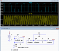
Below is the LTspice simulation of one circuit with the Schmitt NAND gate and the other with three inverting gates.

The NAND gate circuit shows the normal oscillation frequency (≈439kHz) for the shown RC value (blue trace).

The high speed oscillations (≈4.7MHz) with the 3 inverting gates (yellow trace) for the same RC values, illustrates my concern with that circuit with no hysteresis.

upload_2018-11-29_21-50-5.png
 
Last edited:

MrChips

Joined Oct 2, 2009
30,794
I put the 4049 triple-inverter circuit on a breadboard with R1 = 2kΩ, C1 = 1nF, Vdd = 5V.
Oscillation is square wave at 205kHz 50% duty cycle.
 

crutschow

Joined Mar 14, 2008
34,407
I put the 4049 triple-inverter circuit on a breadboard with R1 = 2kΩ, C1 = 1nF, Vdd = 5V.
Oscillation is square wave at 205kHz 50% duty cycle.
So apparently there's sufficient hysteresis in a real circuit to avoid the problem the simulation shows.
 
Top