Hello all,
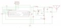
I am a wildlife biologist with a strong interest in the use and development of radiotelemetry devices for use in tracking small animals. A few months ago I wrote a post about getting help with analyzing a circuit of one of the world's smallest VHF radiotags (see attached circuit diagram and this post) for a species of bird that I work with in the Neotropics; a design published by Naef-Daenzer and others (2005).
Over the last few months I have moved from this simple RC-pulsed design to a similar design, but where the RF pulses are controlled by an MCU. Although I have already gotten a circuit working using an ATtiny20 MCU, the transmissions have completely detuned (i.e. the harmonic filtering that led to a strong emphasis of the 3rd harmonic [144 MHz] in the original analog design no longer results in any appreciable filtering of the fundamental, or any other harmonics).
The changes I've made to the design are fairly modest. WRT the attached circuit I have removed R1 (replaced it with a short), replaced R3 with a N-channel MOSFET to serve as a low-side switch, and attached the MCU to VCC, GND, and one I/O to the gate of the FET. Although the circuit works fairly well otherwise, the detuning of the RF carrier has made the transmitter useless in its current form.
I have been consulting with three very bright electronics students at my university, and one of them suggested that the parasitic capacitance and/or the on-state resistance of the FET (~250 milli Ohm) could interfere with the harmonic filtering of the RF oscillations. I have tested the circuit's harmonic output using a manual switch (replacing the FET) to control output, and the harmonics are filtered as intended (I believe that result lends further evidence for the idea that the problem is causally linked to the FET).
First, does this sound like a reasonable diagnosis of the tuning problem? If so, does anyone out there have any suggestions for 1) a location where the FET could be moved where it would not interfere with the RF carrier (possibly using a high-side switch instead)? or 2) passives that could be inserted to isolate the parasitic effects of the FET from the RF output of the BJT (e.g. reinserting R3 so that it lies between the BJT and the FET)?
Any advice or knowledge you could offer for any of these questions would be greatly appreciated!
Many thanks,
Julian
Attachments
-
 159 KB Views: 22