 Facebook
 Google
 GitHub
 Linkedin
Hello all,
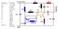
This is my first post on this forum, but likely not the last. I am a wildlife biologist with a strong interest in the use and development of radiotelemetry devices for use in tracking small animals. Although I have developed a strong interest in RF circuit design, I am still far from proficient. Over the last few years I have been working with and modifying a design of one of the world's smallest VHF radiotags (see attached circuit diagram) for a species of bird that I work with in the Neotropics; a design published by Naef-Daenzer and others (2005).
For a number of years the Naef-Daenzer tag was sufficient for my needs, and I didn't need to understand the circuit itself to use it. However, I am now interested in moving from this simple RC-pulsed design to a similar design, but whose RF pulses are controlled by an MCU. Although I have already gotten a circuit working using an ATtiny20 MCU, I would like to have greater understanding of the different components of the Naef-Daenzer circuit so that I can identify and then remove unnecessary components, and modify others (such as matching and filtering networks). What I have gleaned from communication with Naef-Daenzer himself, his paper, and my own limited understanding of electronics, I have been able to identify components that deal with smoothing input voltage and limiting output amplitude (purple components in diagram), those generating/modifying the pulses (blue), those responsible for RF generation and amplification (yellow), and those involved in RF filtering (red). I have tried to simulate this circuit with PSPICE, but have had little luck getting it to work, although an AC sweep analysis with an AC source in place of Q does reveal strong resonance at ~203 MHz, which is NOT the frequency produced by this tag [i.e. 148.5 MHz]).
My questions, for anyone willing and able to help point me in the correct direction are the following:
1) What is the function of R2, L1, L2, and C3 in this circuit? Do these appear to be involved in impedence matching and filtering, or are they related to the feedback required for running the oscillator? Generally, how are they operating?
2) L3, C4, and C5 are supposedly a "pi-filter-like matching circuit," for the 148.5 MHz frequency of the tag. Can anyone explain how this filter operates, given that it is not exactly a pi filter? How can I calculate the hypothetical cut-off frequency for it? Is it possible to modify the values of C and L to operate on a different frequency (e.g. on the 166.38 MHz band), or would a completely different matching network be required?
Any advice or knowledge you could offer for any of these questions would be greatly appreciated!
Many thanks,
Julian
Attachments
-
 159 KB Views: 45


