Understand Circuit (newbie) -- old clock radio with digital chip, TI -- TMS3450NL

Thread Starter

dw85745

Joined Oct 5, 2015
32
I understand what each electronic component does, I'm now trying to understand how they are used in a circuit.
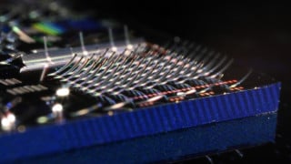
I have this old clock radio I'm using as a basis on understanding.
If has a analog side (power) and digital side (chip by TI -- TMS3450NL)
Page 10 of the attached file is the general overview of its working with more details in pages 1 to 9.
QUESTIONS (a lot):

1) I understand there is a analog signal coming off the transformer secondary supply the power at 60 Hz (since I'm in the US.
I also assume this analog wave is a sine wave since that is what should be generated by the power company.
Question: Why are they running this feed though a resistor before it gets to the chip ?

2) It appear the return to the transformer (Vss) is just the negative part of the sine wave.
The positive portion (Vdd) of the wave is being being looped back to the primary input (60 Hz)
I get why the diode is there (to block the primary wave feeding the chip on the Vdd side)
Question: Why the electrolytic cap, and diode between Vss and Vdd and also why the resistor
on the Vdd line between the two?.
 

Attachments

MrChips

Joined Oct 2, 2009
30,795
With reference to the circuit schematic shown below:

Question: Why are they running this feed though a resistor before it gets to the chip ?
This is not essential since the input current is 10μA max, but provides some circuit protection.

Question: Why the electrolytic cap, and diode between Vss and Vdd and also why the resistor
on the Vdd line between the two?.

This circuit is an AC-to-DC power rectification circuit. The capacitor is called a reservoir capacitor and its purpose is to smooth out the supply voltage in between 50/60Hz line peaks.
The diode between Vss and Vdd is a zener diode which is used to regulate the output voltage of the DC supply. The resistor limits the current to the zener diode. Without this resistor the zener diode would blow.
TMS3450NL Clock.jpg
 

dl324

Joined Mar 30, 2015
16,911
Schematic of circuit in question:
upload_2018-8-31_7-42-26.png
Question: Why are they running this feed though a resistor before it gets to the chip ?
Current limiting.
Question: Why the electrolytic cap, and diode between Vss and Vdd and also why the resistor on the Vdd line between the two?.
The resistor establishes the zener current, the capacitor filters the supply voltage, the diode blocks the half cycle that would forward bias the zener and discharge the capacitor.
 

Thread Starter

dw85745

Joined Oct 5, 2015
32
Thanks you for both responses.
In my own words -- hopefully correct --and followup;
Re 1:
The transformer secondary will determine the amount of current.
By adding the resistor, this ensures that "that current value" does not exceed the design maximum.

Followup on the #2:
Re Capacitor Filtering and Smoothing out the supply voltage.
So if I was able to look at this wave would I see a 60 Hz sine wave where the
+/- amplitude is limited to some range, - or - would the top and bottom wave peaks be clipped (flat)?

Re: Zenor Diode and regulating the output voltage.
Why is the voltage regulated on the output side and Not the input side?
 

Thread Starter

dw85745

Joined Oct 5, 2015
32
Time ran out for Edit:
My understanding all Chips are DC powered. So since this chip is receiving an AC input is their
an AC/DC convertor built internally within the chip?
 

Dodgydave

Joined Jun 22, 2012
11,302
Time ran out for Edit:
My understanding all Chips are DC powered. So since this chip is receiving an AC input is their
an AC/DC convertor built internally within the chip?
No, if you're referring to the resistor from the transformer to the 50/60Hz pin, this is used as the Clock signal for the timbase, rather than using an Xtal oscillator.
 

Thread Starter

dw85745

Joined Oct 5, 2015
32
Dodgydave:

I'm really confused now.
I have an analog signal from the transformer and a resistor that is providing protection.
I can so see that the 60Hz cycle could be used as a clock instead of having a Xtal.
But how is the AC being converted to DC ?
=== AND -===
if the Chip is AC not DC why the DC out on the right side of the schematic?
 

MrChips

Joined Oct 2, 2009
30,795
The chip operates on DC.

The 60Hz signal is AC going into the chip. This is used as a stable and accurate signal for time-keeping purposes. The AC signal is rectified internally by the chip so that only one-half of the 60Hz cycle is used to pulse the internal timers of the chip. You do not have to be concerned with how this is done in the chip.
 

Thread Starter

dw85745

Joined Oct 5, 2015
32
MrChips: Thanks. That makes sense.
so:

1) On the analog side
The Vss (negative part) of the 60 cycle is being returned AS IS to the transformer second..
The Vdd (positive part) is being re-injected into the 60Hz supply. (I'm guessing no phase shift) as well as portion of the Vdd passing through the zener to marry up with the Vss to return to the second.
Getting back to the zener regulation of the output voltage, I'm guessing it does not matter whether you regulated the AC voltage on the input or output side as long as it is regulated?
2) It also appears some portion of the AC is also flowing through the chip and back to the second via Cycle1 and Cycle2 connected to the LED display.
3) Where is the ground side of the DC?
 
Last edited:

BobaMosfet

Joined Jul 1, 2009
2,113
@dw85745
You have 4 components on your Vss & Vdd rails. A diode which clips the 60Hz whole-cycle to a half-cycle. This charges the capacitor. The resistor limits current to the zener and into the chip. The zener controls the voltage level. And during the portion of the A/C sine wave that is clipped (doesn't exist in DC-land), the capacitor then provides power during that period. Once again, the resistor comes into play to limit how quickly the capacitor empties itself.

That is how A/C is converted to DC in this circuit. Vss is ground, Vdd positive rail.
 

Thread Starter

dw85745

Joined Oct 5, 2015
32
I can see where the diode could clip the 60Hz cycle to half cycle.
But the Vdd coming from the second should be a full 60 cycle, and as the diode is pointing toward the Vdd, flow would be in that direction.
and hence it would be combined with the full 60Hz.entering the chip through the 50/60Hz pin
-- OR --
???
 

MrChips

Joined Oct 2, 2009
30,795
You are over-thinking this problem. The drawing is not a complete circuit diagram but only to give the designer a sense of how the chip is used.

The 50/60Hz input only takes 10μA. Hence only a very light coupling to the AC mains is required.

TMS3450 is a MOS P-channel device. Ground is Vdd on pin-20. Vss on pin-15 is positive polarity.
 

Thread Starter

dw85745

Joined Oct 5, 2015
32
Timed out on my -- OR -- response again.
Rereading BogaMosfet's response - if understanding correctly
It makes sense that the DC supply is entering the chip through the Vdd.
However, how is the AC returned to the secondary that is entering through the 50/60Hz pin?
 

Thread Starter

dw85745

Joined Oct 5, 2015
32
Mr.Chips:
1) You are over-thinking this problem. The drawing is not a complete circuit diagram but only to give the designer a sense of how the chip is used.
Probably over-thinking. I have the actual clock with PCB and looking at the PCB same components are there as per diagram except a coil has been added. Haven't confirmed traces to components per diagram but most probably the same.

2) Get that Vss or Vdd is supply. Little confused over your comments and BobaMosfet's response
regarding whether Vss or Vdd is the supply rail?
Found this which helps:
LinK: https://forum.allaboutcircuits.com/threads/what-is-vcc-vss-vdd-vee.28782/
They are all supply voltages. Vcc = Collector supply voltage, Vee = Emitter supply, Vdd = Drain supply, Vss = source supply.

The voltages can be negative or positive depending on the the device and the circuit configuration. In circuits using NPN transistors Vcc is generally positive but if you were using PNP transistors then Vcc would be negative. In a circuit with a mixture of PNP and NPN devices Vcc take the polarity of the predominant technology used (generally it would be positive).
 
Last edited:

Dodgydave

Joined Jun 22, 2012
11,302
Dodgydave:

I'm really confused now.
I have an analog signal from the transformer and a resistor that is providing protection.
I can so see that the 60Hz cycle could be used as a clock instead of having a Xtal.
But how is the AC being converted to DC ?
=== AND -===
if the Chip is AC not DC why the DC out on the right side of the schematic?
Here is a working circuit from the datasheet, and you can see the chip uses a 50/60Hz (pin 25) clock input from the transformer secondary, this is just a set pulses to keep the clock timebase accurate, the return path for the pulse will be pin 26,. The normal supply +/- is on pins 20,15.
TMS3450NL_Clock_schematic.png
 

Thread Starter

dw85745

Joined Oct 5, 2015
32
DodgyDave:
That helps a bunch. Also confirms what Mr. Chips had to say.
Will take a bit to study diagram and post back.

Thanks to All for all your efforts on my behalf.

David
 

MrChips

Joined Oct 2, 2009
30,795
Remember, supply rail is relative. I doesn't really matter which side you call GND. One side is more positive than the other.
In this case, since this is P-type MOS fabrication, we can think of one side being more negative than the other.
VDD, pin-20 is more negative that VSS, pin-15.
 

Thread Starter

dw85745

Joined Oct 5, 2015
32
Had a holiday weekend so took some time and reviewed what each component does in AC versus DC circuits.
Next annotated the schematic with arrows to identify where the AC routes (as I see it).
Based on my understanding of elecronics to date, this chip is powered by AC as I sure don't see where it is converted to DC.
The two small tailed arrows at the bottom of the schematic -- that route to the transformer from CATH1 and CATH2) might be DC (???) if something converted it inside the IC.

One of the questions I did have is what happens to the AC when it goes head to head. For example the AC routes from the transformer to the cathode part of the
diode (D3) where it should be stopped (see note "ac halt"). However the ac traces also wrap such that they feed this same diodes anode (D3) where it should pass through the diode and continue back to the 6 volt (supply) on the transformer.. Is the ac impacted in anyway when it encounters the other ac on the cathode also from that 6 volt supply?
 

Attachments

Last edited:
Top