Unable to stop current flow through an enhancement mode P-Channel MOSFET

Thread Starter

ogre2724

Joined Aug 23, 2016
9
Hey all, first time on this wonderful site. I've looked around quite a bit and can't seem to find anything that points out an obvious answer to this issue I'm having...

I'm trying to create a power switch to some external circuitry. The external circuitry is run off of a 12Vdc supply and draws around 200 mA, peaking around 300 mA for short bursts (~1ms) when operating, but is brought down to roughly 1mA with small spikes of 100mA when I bring it to shutdown.

I must control this switch through a digital output pin, setting it 1 turning the circuitry on, and 0 for off.

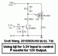
After looking through The Art of Electronics, I decided to employ the circuit attached below as my power switch.

It is supposed to utilize an NPN BJT employed as a current sink from my digital output pin to control the voltage present at the gate of the PMOS, thus allowing current to flow through the 12V supply or stop it completely (or at least drop it to roughly 10nA consumption)...

The load is inductive, and the 12V power supply (once past the PMOS), is fed into this step-down buck converter here:
http://www.ti.com/lit/ds/symlink/tps54229e.pdf

(There is a transient voltage suppressor included in the load that is wired from 12V (just after the Drain of the PMOS) to ground)

The circuit runs perfectly when switched on- Vg is dropped down to roughly 4V, allowing for current to sink to the load.

I'm getting very odd results when trying to switch the circuit off though- Vg is .65 volts... so current is still allowed to sink.

Any help would be MUCH appreciated, and feel free to criticize and ask questions. Fresh undergrad here that's still trying to learn all the tricks!

~William
 

Attachments

wayneh

Joined Sep 9, 2010
17,498
Change the position of Re to above the transistor, so that the emitter is tied to ground. I don't see why you couldn't just eliminate (short) Re.

Add a base resistor in between the output and the base of the transistor, to protect your digital output to well under it's maximum current. Any value between 47K and 470K should be fine to maintain full function. If you care about the current there, you could experiment with higher values.

On the other hand, I'd be tempted to use a 10K or lower for Rc. Then use a base resistor that is roughly Rc•10. Again assuming there is no Re.

High gate resistor values (like your 56K) increase the time to charge/discharge the gate capacitance. The MOSFET can get hot when it has an intermediate gate voltage between full on or full off. So you generally go as low as you can without causing excessive currents in that tiny time period of charging or discharging.
 
Last edited:

Thread Starter

ogre2724

Joined Aug 23, 2016
9
Change the position of Re to above the transistor, so that the emitter is tied to ground. I don't see why you couldn't just eliminate (short) Re.

Add a base resistor in between the output and the base of the transistor, to protect your digital output to well under it's maximum current. Any value between 47K and 470K should be fine to maintain full function. If you care about the current there, you could experiment with higher values.

On the other hand, I'd be tempted to use a 10K or lower for Rc. Then use a base resistor that is roughly Rc•10. Again assuming there is no Re.

High gate resistor values (like your 56K) increase the time to charge/discharge the gate capacitance. The MOSFET can get hot when it has an intermediate gate voltage between full on or full off. So you generally go as low as you can without causing excessive currents in that tiny time period of charging or discharging.
Hello wayneh, thanks for the reply.

I've made the following changes that you've suggested to me- Removed the Re, changed Rc to 10k, and changed Rb to 100k.

When turned on, the PMOS supplies current perfectly still, but when set Vb to 0, the current sinks through the PMOS still, because the gate voltage stays low at .7 Volts... Isn't the gate voltage suppose to be matched to the Source voltage to stop current flow? Should I just be using an NMOS instead? Was the NPN transistor I chose a little weird? How about the PMOS QFET? I know QFET only means it's extremely fast at charging and discharging... but maybe there are some other properties I'm missing on it.

Thanks again for your response though,
~William
 

ian field

Joined Oct 27, 2012
6,536
Hey all, first time on this wonderful site. I've looked around quite a bit and can't seem to find anything that points out an obvious answer to this issue I'm having...

I'm trying to create a power switch to some external circuitry. The external circuitry is run off of a 12Vdc supply and draws around 200 mA, peaking around 300 mA for short bursts (~1ms) when operating, but is brought down to roughly 1mA with small spikes of 100mA when I bring it to shutdown.

I must control this switch through a digital output pin, setting it 1 turning the circuitry on, and 0 for off.

After looking through The Art of Electronics, I decided to employ the circuit attached below as my power switch.

It is supposed to utilize an NPN BJT employed as a current sink from my digital output pin to control the voltage present at the gate of the PMOS, thus allowing current to flow through the 12V supply or stop it completely (or at least drop it to roughly 10nA consumption)...

The load is inductive, and the 12V power supply (once past the PMOS), is fed into this step-down buck converter here:
http://www.ti.com/lit/ds/symlink/tps54229e.pdf

(There is a transient voltage suppressor included in the load that is wired from 12V (just after the Drain of the PMOS) to ground)

The circuit runs perfectly when switched on- Vg is dropped down to roughly 4V, allowing for current to sink to the load.

I'm getting very odd results when trying to switch the circuit off though- Vg is .65 volts... so current is still allowed to sink.

Any help would be MUCH appreciated, and feel free to criticize and ask questions. Fresh undergrad here that's still trying to learn all the tricks!

~William
Someone else answered your question - the symbol you've drawn indicates a depletion type FET, I'm guessing you meant to indicate an enhancement type.
 

Thread Starter

ogre2724

Joined Aug 23, 2016
9
Short the gate to the source.
That should turn the MOSFET off.

Yes, but then there is no way to turn the gate on. And I've confirmed in tests that the current is completely stopped when the Vg = Vs. I need to find a way to get Vg = 12V when my digital output pin is 0V (low). Thanks for the responses everyone.

Also, yes it is meant to be an enhancement mode P-channel MOSFET. Sorry that's how it was drawn in my book here. :/
 

Thread Starter

ogre2724

Joined Aug 23, 2016
9
I have also have some MCP1407 IC's that are MOSFET gate drivers, but I'm not finding too much success with operating them at all. Am I suppose to run their output directly to the load? Or should the output go to the base of an N-channel, enhancement mode MOSFET?

Thanks everyone for your patience
 

GopherT

Joined Nov 23, 2012
8,009
I have also have some MCP1407 IC's that are MOSFET gate drivers, but I'm not finding too much success with operating them at all. Am I suppose to run their output directly to the load? Or should the output go to the base of an N-channel, enhancement mode MOSFET?

Thanks everyone for your patience

WP_20160824_001.jpg
 

Alec_t

Joined Sep 17, 2013
14,312
If Gopher's circuit doesn't do the trick you could try adding a 10k pull-down resistor from the BJT transistor base to ground, in case the Arduino output isn't pulling all the way to ground.
 

ian field

Joined Oct 27, 2012
6,536
Stupid question: Are the grounds of the circuit supplying the 3.3V signal and the 12V supply connected together?

Bob
The KSD261 in the TS's sketch is a manufacturer specific version of the 2SD261 - which is more or less a medium power transistor.

It shouldn't do any harm, but it'd have slightly higher leakage if operated close to its VCEmax.
 

BobTPH

Joined Jun 5, 2013
8,938
The KSD261 in the TS's sketch is a manufacturer specific version of the 2SD261 - which is more or less a medium power transistor.

It shouldn't do any harm, but it'd have slightly higher leakage if operated close to its VCEmax.
Well, he supposedly tried a 10K resistor and got 0.7V on the collector with a 12V supply. That would be (12-0.7) / 10000, which is over 1mA. That is a lot of leakage for a turned off transistor.

Bob
 

AnalogKid

Joined Aug 1, 2013
11,036
I would reduce Rgs (R3 in the post #14 schematic) to something between 1K and 10K to provide a much more firm pull up that is less susceptible to external noise and leakage currents. Also, delete R4.

It sounds like the driver transistor is not turning off. Are you sure it still is functioning after being operated without a base current limiting resistor?

ak
 

ian field

Joined Oct 27, 2012
6,536
I would reduce Rgs (R3 in the post #14 schematic) to something between 1K and 10K to provide a much more firm pull up that is less susceptible to external noise and leakage currents. Also, delete R4.

It sounds like the driver transistor is not turning off. Are you sure it still is functioning after being operated without a base current limiting resistor?

ak
What's the Vout low on the Arduino shield?
 

Thread Starter

ogre2724

Joined Aug 23, 2016
9
Tried the circuit posted from GopherT above, still having issues. I've found the issue stems from the fact that I'm still sinking current through the BJT even when I want it switched off. I think it's because of the type of transistor I previously purchased, so I'm switching out to the standard 2N9304 from Fairchild to see if the base current doesn't always conduct even when in the mV range of my digital output being put low.

What's the Vout low on the Arduino shield?
It's around 2mV.

Also, do you guys think using an optocoupler might be a good idea to completely isolate the electrical signal from the digital pin from the load I'm driving? Or do you guys think the same issue of the PMOSFET not being able to turn off might occur?

Also, since there is already a TVS applied around the load that I'm driving, will adding an RC snubber in parallel do any good?

Really not liking working with inductive loads right now... Thank you all for your help so far though.

~William
 

Thread Starter

ogre2724

Joined Aug 23, 2016
9
I would reduce Rgs (R3 in the post #14 schematic) to something between 1K and 10K to provide a much more firm pull up that is less susceptible to external noise and leakage currents. Also, delete R4.

It sounds like the driver transistor is not turning off. Are you sure it still is functioning after being operated without a base current limiting resistor?

ak
What about those values makes it susceptible to external noise and leakage currents? Genuinely curious as I'm trying to learn more about these switches and the nuances of them... :)

And although it does seem like the transistor isn't turning off, it's basically off... I measured the current draw through the resistors of the base and collector resistors and they were drawing merely nano amps. However when I hooked up my o-scope probe across Rc, the entire behavior of the circuit completely changed (probably because of the added 13pF capacitance added in parallel to Rc from the probe itself) but I'm wondering if this is a red flag telling me, "Hey, this circuit is super unstable, even if you manage to get the switch working correct."

Thanks again
 

Thread Starter

ogre2724

Joined Aug 23, 2016
9
Also for this P-channel MOSFET, keep in mind it's a Power MOSFET, so the body is connected to the something... Don't know if that's significant to how pushback current is allowed to travel around my circuit back to Vg in some manner... Thanks.
 

ian field

Joined Oct 27, 2012
6,536
Tried the circuit posted from GopherT above, still having issues. I've found the issue stems from the fact that I'm still sinking current through the BJT even when I want it switched off. I think it's because of the type of transistor I previously purchased, so I'm switching out to the standard 2N9304 from Fairchild to see if the base current doesn't always conduct even when in the mV range of my digital output being put low.


It's around 2mV.

Also, do you guys think using an optocoupler might be a good idea to completely isolate the electrical signal from the digital pin from the load I'm driving? Or do you guys think the same issue of the PMOSFET not being able to turn off might occur?

Also, since there is already a TVS applied around the load that I'm driving, will adding an RC snubber in parallel do any good?

Really not liking working with inductive loads right now... Thank you all for your help so far though.

~William
Are you sure its only 2mV?! - it seems unlikely as many logic families only guarantee Vout low not higher than about 800mV.

If the bipolar transistor isn't letting go all the way up to Vcc; its either taking base current or faulty (leaky).

You could try replacing the bipolar with a TO92 style MOSFET like the 2N7000 etc - it has a VGSthr in the range 0.8 - 3.0V. Personally; I'd go for a regular TO220 style logic level MOSFET - I frequently use over-capable MOSFETs because their other electrical characteristics are *CONVENIENT*.

There are probably less good TO92 MOSFETs if you could be bothered searching them out - something with a 2V minimum VGSthr should work OK.
 
Top