Trying to understand why 555 timer is configured this way when reverse engineering a IR transmitter

Thread Starter

robnoper

Joined Mar 5, 2019
24
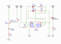
I have reverse engineered a IR transmitter that im going to incorporate in my own design and PCB

For those of you who are far more knowledgeable than I am, can you let me know what purpose the diodes and transistors form in this circuit.
The original board had surface mounted components and believe the original diodes are Glass Zener diodes with a pale blue stripe and no other markings.

The transistors are marked as below. The circuit is gets 9v through a voltage regulator.

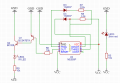
On the next board I want to reproduce are some SMC transistors, marked "W1P84" any idea what they could be.
upload_2019-5-7_8-40-46.png

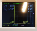
This is the scope output from pin 3 of the 555 before the transistors.
upload_2019-5-7_8-44-15.png

And this was from pin 6 I believe

upload_2019-5-7_8-44-53.png
 

Attachments

LesJones

Joined Jan 8, 2017
4,174
I think you have missed the timing capacitor from your schematic. Also I think you have the wrong value for R9. I would expect it to be a low value to give large current pulses through the IR LED. The two transistors just amplify the output from the 555 to give the short large current pulses through the IR LED. I don't understand why the two displays on your are not showing the same frequency.

Les.
 

Thread Starter

robnoper

Joined Mar 5, 2019
24
I think you have missed the timing capacitor from your schematic. Also I think you have the wrong value for R9. I would expect it to be a low value to give large current pulses through the IR LED. The two transistors just amplify the output from the 555 to give the short large current pulses through the IR LED. I don't understand why the two displays on your are not showing the same frequency.

Les.
Sorry yes your right missed of the capacitor...will adjust and re-post
 

jpanhalt

Joined Jan 18, 2008
11,087
Are you assuming the circuit as drawn is correct and works? We know it is missing the timing capacitor, and that generally connects to trigger and threshold.
 

BobaMosfet

Joined Jul 1, 2009
2,110
Q1 is open-collector and has no pull-up/pull-down resistor to help control base on Q2 (it needs one). Together Q1 and Q2 invert the signal and amplify it.
 

Thread Starter

robnoper

Joined Mar 5, 2019
24
Yes this is with the capacitor added.

Any feedback on the Surface Mounter Transistor "W1P84"

That will be the next thing i move on to.
upload_2019-5-7_19-59-10.png
 

Thread Starter

robnoper

Joined Mar 5, 2019
24
Q1 is open-collector and has no pull-up/pull-down resistor to help control base on Q2 (it needs one). Together Q1 and Q2 invert the signal and amplify it.
Thanks for your feedback and will look at this.. What would be the benefit/reason for inverting the signal? Amplifying it will give it more power?
 

Thread Starter

robnoper

Joined Mar 5, 2019
24
Are you assuming the circuit as drawn is correct and works? We know it is missing the timing capacitor, and that generally connects to trigger and threshold.
Yes thankfully its reasonably simple and works. Trying to understand why they have done the things this way so i can learn more.

This is the original board. There are two capacitors a diode and a 9v voltage regulator bottom left but i dont need that i dont think. I get that from the circuit im joining this to.

upload_2019-5-7_20-4-46.png
 

jpanhalt

Joined Jan 18, 2008
11,087
Have you built that circuit as you show it? There many by an error in how pins 2 and 6 are connected. The circuit I posted along with some variations is pretty standard.

As you say, "it works," so no argument. You can trace the charge and discharge pathways. The principle that the diodes act as "steering" devices still holds to get duty cycles less than 50%.
 

Polymorph

Joined Feb 6, 2009
6
Is there a reason you've drawn this schematic upside down and backwards?

Usually, ground is at the bottom, Vcc at top, input on the left, output on the right.

I prefer drawing a 555 timer as a diagram, not as a pictorial element. It makes it simpler to understand what is happening.

upload_2019-5-9_20-18-16.png
Pin 7 is the discharge pin. Pins 2 and 6 are !Trigger and Threshold. Pin 3 is the Output. Pin 4 is Vcc, pin 1, is ground, pin 8 is !Reset. Pin 5 is a Control voltage input.
upload_2019-5-9_20-20-40.png
 
Top