 Facebook
 Google
 GitHub
 Linkedin
I am interested in making an animal microchip reader out of arduino. In Australia, all the transponder in animals are 134.2kHz and use fdx-b (full duplex ASK modulation).
I found this Post from arduino playground(https://playground.arduino.cc/Main/DIYRFIDReader) and it's linked forum post, and therefore confident this circuit works for my intended purpose as well.
While I can certainly use the circuit as is, I really want to know how it works as well. My previous projects all involve using IC appropriate for the job, therefore components I ever really added to my previous circuits are just load resistors, decoupling capacitor, inputs and switches.
I may not have formal education on electrical and electronics, but I have done a lot of research on past weeks just trying to make sense of this circuit but I still fail, therefore I am asking for help.
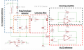
Attached is a copy of the circuit you can find in the post mentioned above, with my understanding of how it works.
With that I have following specific questions:
1. What is the purpose of D2 and ground at that position? What's the difference if such ground does not exist? Shouldn't current flow through pin 9 when it is low anyway?
2. All the example I have seen regarding peak/ envelope detecting circuit has diode towards the stage instead of opposite like D1, therefore I simply cannot imagine how currents flow through here, and how/when current pass through the diode D1.
3. what is C2 doing when there is C3? In my understanding that's where the signal is pass on to the next stage, and C3 with R1 is a peak detector already?
4. I don't really understand how the modulated signal can be decoupled from the carrier wave. I understand the modulated signal will be of much lower voltage, but as far as I understand, low pass filter filter out high frequency wave, not high voltage (amplitude?) wave, so how was it achieved?
5. What is the purpose of having voltage follower and R5 right after it in the Vcc/2 reference there? the upstream (input) is feeding into earth anyway, and downstream (output) is feeding into another op amp which has high impedance and virtually no current flow through it. What's the point of a voltage buffer when it is likely very stable? The load right after it makes even less sense to me as shouldn't it makes the voltage drop and defeat the purpose of the voltage buffer?
Sorry if it is too many questions at once, but I really hope to understand how it works, and there is really limited resources on the web explaining rfid circuits.
I found this Post from arduino playground(https://playground.arduino.cc/Main/DIYRFIDReader) and it's linked forum post, and therefore confident this circuit works for my intended purpose as well.
While I can certainly use the circuit as is, I really want to know how it works as well. My previous projects all involve using IC appropriate for the job, therefore components I ever really added to my previous circuits are just load resistors, decoupling capacitor, inputs and switches.
I may not have formal education on electrical and electronics, but I have done a lot of research on past weeks just trying to make sense of this circuit but I still fail, therefore I am asking for help.
Attached is a copy of the circuit you can find in the post mentioned above, with my understanding of how it works.
With that I have following specific questions:
1. What is the purpose of D2 and ground at that position? What's the difference if such ground does not exist? Shouldn't current flow through pin 9 when it is low anyway?
2. All the example I have seen regarding peak/ envelope detecting circuit has diode towards the stage instead of opposite like D1, therefore I simply cannot imagine how currents flow through here, and how/when current pass through the diode D1.
3. what is C2 doing when there is C3? In my understanding that's where the signal is pass on to the next stage, and C3 with R1 is a peak detector already?
4. I don't really understand how the modulated signal can be decoupled from the carrier wave. I understand the modulated signal will be of much lower voltage, but as far as I understand, low pass filter filter out high frequency wave, not high voltage (amplitude?) wave, so how was it achieved?
5. What is the purpose of having voltage follower and R5 right after it in the Vcc/2 reference there? the upstream (input) is feeding into earth anyway, and downstream (output) is feeding into another op amp which has high impedance and virtually no current flow through it. What's the point of a voltage buffer when it is likely very stable? The load right after it makes even less sense to me as shouldn't it makes the voltage drop and defeat the purpose of the voltage buffer?
Sorry if it is too many questions at once, but I really hope to understand how it works, and there is really limited resources on the web explaining rfid circuits.
Attachments
-
 314.9 KB Views: 20


