Traffic generation in virtex-7 fpga using Xilinx MIG

Thread Starter

rahdirs

Joined May 22, 2013
28
Problem: I have data sampled in an ADC at 337.5 MHz(actually it is sampled at 1335 MHz,but for sake of DDR3RAM i am slowing down the rate at which data comes out,using 1:2 demux provided within ADC) which needs to be written to a DDR3 RAM via a Virtex 7 fpga.(I am using Xilinx Vivado Design Suite)

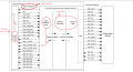
My progress: To write data from Virtex 7 to DDR3 RAM, i used memory controller ip core given by vivado tool.After designing this,i need to give data from ADC to this memory controller module(some sort of interface).

So my question is, 1) can i use traffic generator provided by Xilinx for my purpose or do i need to write a new traffic generator for my purpose ?
2) Even with traffic generator i would require a user interface or the example traffic generator itself is sufficient ?
 

Papabravo

Joined Feb 24, 2006
21,094
That is not much to go on. You might start with a description of what a traffic generator is supposed to do and why or why not the one provided by Xilinx might or might not be suitable.
 

Thread Starter

rahdirs

Joined May 22, 2013
28
You might start with a description of what a traffic generator is supposed to do and why or why not the one provided by Xilinx might or might not be suitable.
Traffic generator is a module that generates/determines which address location to write into in a ddr3,generates/routes data patterns to ddr3 etc...
As to why it may not work,it will work but i think it will involve modifying their code for my purpose which may take a lot of time.

When i searched around in google, i found a lot of ppl working on traffic generators etc..,so was trying to get their advice on how they do it(either modifying xilinx's code/writing their own traffic generator).
 

Papabravo

Joined Feb 24, 2006
21,094
What you are describing sounds like a DMA controller. This was a device that ran in parallel to a CPU and allowed I/O data from a device to be read from or written to memory. It had to generate addresses, request access to the memory bus, run the memory bus cycle, and then relinquish the bus. In your case will the ADC samples be placed in successive locations or will they be scattered according to some pattern for later recovery.
 
Last edited:

Papabravo

Joined Feb 24, 2006
21,094
So designing it yourself will get you exactly what you want instead of having to understand an debug somebody else's design. I've always found this the best way to go. Of course you can look at the library version to see if there are any clever ideas there.
 

Thread Starter

rahdirs

Joined May 22, 2013
28
My intention: I have data sampled in an ADC.I want to write that data into DDR3RAM using Virtex-7 fpga.(Why ?) use fpga is it is an existing architecture and there is no direct interface between adc & ddr3ram & i can't change design at this stage.

Now this is how i understood the problem.Refer figure1 which shows 7 Series FPGAs Memory Interface Solution from Xilinx User Guide.I've added some names on interface. Are they correct ? And can i have my user interface in figure1(which i wrote as figure2) implement the state diagram of figure 2 ?
 

Attachments

Papabravo

Joined Feb 24, 2006
21,094
From the information provided I cannot answer your question. This is one of the problems with a provided solution. Without a great deal of conversation with a Xilinx App Engineer or someone who has used it before you just don't know if it will meet your needs. Is it possible that you can run a quick test to determine the suitability? What is the cost(penalty(?)) of deciding to use it and finding a flaw in the design for your purposes.
 
Top