Thoughts on a high frequency function generator.

Thread Starter

RichardO

Joined May 4, 2013
2,270
There has been enough drift in another thread that I think it makes sense to start another one. See:
https://forum.allaboutcircuits.com/threads/op-amp-oscillates-with-gain-in-feedback.141128/

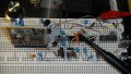
To recap. I am building a very high frequency function generator. The original thread was asking for help in getting the current source that charges and discharges the timing cap working.

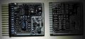
With that help I was able to make a PCB to do some testing.

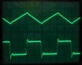
To keep thing coherent I have attached the pictures of the breadboard again.

View attachment 139474 View attachment 139475 View attachment 139476

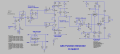
Here is the LTspice simulation of what I have on the solderless breadboard:
upload_2017-11-16_11-19-5.png
upload_2017-11-16_11-19-32.png
 

Attachments

Thread Starter

RichardO

Joined May 4, 2013
2,270
There is a lot of frequency bobble at low frequency settings. It appears that the bobble is caused by oscillation on the output of the flip-flop when it changes state.

This should not be possible. My thinking right now is that it might be caused by the outputs of the voltage comparator changing too slowly. Again, this should not matter since once the flip-flop changes state it can't change back until the other peak of the triangle wave. It might be caused by ringing on the breadboard but I don't think, so at this time.

I will be looking at this in more detail to pin down the cause.
 

OBW0549

Joined Mar 2, 2015
3,566
Nevertheless, you're looking pretty good at 10 MHz; I think it's the next decade that will prove the real challenge. I think pretty soon you'll have to go to a PCB with ground plane...
 

Thread Starter

RichardO

Joined May 4, 2013
2,270
Nevertheless, you're looking pretty good at 10 MHz; I think it's the next decade that will prove the real challenge. I think pretty soon you'll have to go to a PCB with ground plane...
I may be able to forestall making a large PCB by making another plugin board with the flip-flop and comparator on it. That would be a PCB with a ground plane.
 

Thread Starter

RichardO

Joined May 4, 2013
2,270
I realized that the flip-flop could be converted from a DIP to a SIP. :D All of the pins I need are on one side of the package and the pins on the other side can be left floating. :)

Since I can "SIPify" the flip flop, I decided that making a hand-wired comparator as a SIP made sense. Doing both of these changes will make the layout of the SBB much more compact. The hand wired comparator SIP has most of the resistors and diodes on it so I expect it to be both faster and have cleaner outputs.

The SIP has the through-hole parts (IC and diodes) on the front side and the SMD resistors on the back side. This made the assembly both fairly easy to do and compact.

3102_dual_comp_f.JPG 3102_dual_comp_b.JPG

I will be testing the board and the new SBB wiring later today.
 

Thread Starter

RichardO

Joined May 4, 2013
2,270
Sounds good.
Status update. Things are progressing...
About the only improvement I can do with the SBB circuit is to put a really high speed op-amp and the parts around it onto a SIP. I have an ADA4817 I might sacrifice to for this use. The 100 MHz current feedback amps just aren't enough. Oh, I just realized that I need to scrounge a MC10H135 to get some improvement in loop propagation delays. I have a friend that is temporarily in California. He might be able to find such a rare beast there.

The latest schematic:
upload_2017-11-21_15-56-59.png
I did a few changes to the circuit -- mostly signal name changes around the CA3102 and MC10135.
- The biggest real change was going from the LM6181 to an EL2030. The EL2030 has slightly larger bandwidth and slightly less delay.
- I added a 3.0 volt Zener for the PECL termination voltage.
- Although it is not shown, I added an LM2940 LDO to get 5.0 volts. Also not shown is a LT1054 charge pump to get the - 5 volts.
- I added pin numbers for the CA3102 and MC10135 to reflect what I did while building the hand-wired comparator SIP. These pinouts only apply to the SBB version of the function generator.

After all of the changes, it still works. At least I didn't break anything. The triangle _may_ be a bit cleaner. This is subjective since I can't compare them side by side. I still only Oscillate at about 15MHz maximum before things start looking screwy. I will take some photos when I get a chance since words are not going to cut it. ;)

I seem to have some kind of oscillation when the frequency pot is set near its minimum. This is about 1/100 of maximum frequency. Only in a small range of the pot setting. :( I suspect that this one is going to be hard to find.

Even though the switcher that creates the 7 volts does not seem to be noisy, I am going to add an inductor to filter its output. I think 10 uH is about right.

There is some ringing or, maybe, reflections on the triangle. I looks like about 75 MHz. I don't expect that I can do much about that on the SBB. The good news is that touching the circuits makes little difference in the frequency or waveforms. In other words, the crumby signals are consistent. :rolleyes:

And finally a picture of what it looks like now:
FG_Handwire_comp.JPG
A lot simpler looking now. :)
Note that the MC10135 that I converted to a SIP is hiding behind the handwired comparator board.
 

Attachments

OBW0549

Joined Mar 2, 2015
3,566
You're really pushing the speed envelope there. Linear Tech's app note An-47 by Jim Williams has a lot of good stuff on high-speed breadboarding techniques. Even 26 years after it was first published, I still refer to it regularly. Good stuff.
 

Thread Starter

RichardO

Joined May 4, 2013
2,270
You're really pushing the speed envelope there. Linear Tech's app note An-47 by Jim Williams has a lot of good stuff on high-speed breadboarding techniques. Even 26 years after it was first published, I still refer to it regularly. Good stuff.
AN-47.... Yes, indeed. I have referenced it many times myself. :D
Some of my avalanche transistor circuit understanding comes from Jim Williams.

If it was easy then it would not be interesting. I have built a lot of circuits on SBB's and have pushed things beyond the envelope. I have the scars to prove it. ;)

I once built a Colpitts oscillator that ran at about 350 MHz. Had to do a lot of tricks to do that. Multiple grounds, bypass, bypass, bypass, shields between contacts, Multi-GHz F_t transistors, bypass, bypass, bypass, some parts were soldered on sub-circuits...

OK, I know what you are thinking. "B......t." I have to add the disclaimer that the 350 MHz was only one of the frequencies I could see. The signal was extremely unstable. Duh. Seemed like a good idea at the time -- what else can I say. Actually, it was a good idea. I learned a lot about limitations -- mostly mine. :D
 

cmartinez

Joined Jan 17, 2007
8,722
A fella could learn a lot about electronics just by reading-- and re-reading-- the collection of his Linear Tech app notes.
One thing I've had to learn the hard way, is the layout techniques for ADC and this sort of high frequency circuits. I know that there's a lot of info on this subject out there, but I've found some or the techniques used so different from one another that they become hard to understand.
 

cmartinez

Joined Jan 17, 2007
8,722
Anything in particular-- or just in general?
The circuit in page 9 in the attached datasheet in particular was a headache to understand a few years ago when I tried to replicate it, trying to build my own high quality ADC. And truth being told, I do not fully understand it yet. I mean, what's the purpose of the 10 ohm resistors (R2, R8 and R9) connecting the analog and digital ground planes on the board? Wouldn't it be best to simply connect the analog and digital grounds to a single point as close as possible to the power supply, as is customary? And why the three power planes under the chip? Is it really that extremely susceptible to noise?

On the other hand, it wasn't until much later that I understood that soldering temp is extremely important when dealing with ADC chips, and that most of my woes stemmed from my unknowingly damaging them during that process, and that those resistors were just a nuisance compared to that.

But most high quality ADC's come in SMT packages. That one in particular has a DIP equivalent, but I couldn't find a single one of them for sale on any of the major available suppliers... It was exactly that experience that taught me that datasheets should be very carefully and thoroughly read before taking any sort of action.

As you already know, I can very well defend myself when dealing with MCUs and digital circuits... but I'm a half-baked amateur when it comes to analog. That is why I always pay close attention to any discussion that you and Richard (and other respectable members, of course) participate on.

Sorry, Richard. I don't mean to veer your thread off course. If you feel I should open another thread for this particular subject let me know and I'll go back to listening mode on this one.
 

Attachments

OBW0549

Joined Mar 2, 2015
3,566
Sorry, Richard. I don't mean to veer your thread off course. If you feel I should open another thread for this particular subject let me know and I'll go back to listening mode on this one.
That's probably the best thing to do, either start a new thread or take it to PM. I'll have to do some noodling about those three resistors; I'm as puzzled as you are.
 

Thread Starter

RichardO

Joined May 4, 2013
2,270
@tindel and obw0549

I have done a lot of changes to the SBB prototype. See here for some background:
https://forum.allaboutcircuits.com/threads/estimating-op-amp-delay.142105/page-2

Here is the list of goals and changes I used:
1) Find source of 235 MHz oscillation.
2) Find source of frequency bobble at low frequency setting.
3) Find source of time asymmetry in sim.
4) Change to 820 ohm resistors in buffer.
5) Add tantalums to Buffer SIP.
6) Add bypass to Dual Comparator SIP. (Including filter caps on bias circuits).
7) Add bypass cap across MC10135.
8) Clean up SBB bypassing.
9) Improve SBB grounding.

Item #1 seems to have been solved. Probably because of better bypassing and reduced gain of the EL2030 circuit.

Item #2 has gone away. I ma not sure why it was there in the first place so it may come back.

Item #3 has not been pursued yet. It may not be a problem in the real hardware which has pots to eliminate asymmetries.

Item #4 was done and the overshoot and ringing are much better. Some delay/bandwidth are sacrificed but that is a good tradeoff right now.

Item 5 is done. I can't believe that I forgot to do that when I first built the circuit. :oops:

Item #6 was done even though I don't think it ahd much effect. Better safe than sorry.

Item #7 was also a belt and suspenders change. ECL is not real noisy.

Items numbers 8 and 9 are ongoing. Much improvement has been done. :D


The triangle looks a lot better -- not as much ringing and n0 235 MHz oscillation is obvious.

The circuit now runs at over 20 MHz but the triangle coming out of the buffer amp is awful. It is much better right on the timing cap.

The triangle is fairly good, but not great, up to 10 MHz.

I will be taking some pictures of the waveforms to post here.

Here is the latest schematic and pictures. (The simulation file is attached).
AAC_FG_SBB_3.JPG AAC_FG_SBB_3_back.JPG AAC_FG_SBB_3_front.JPG upload_2017-12-3_14-58-17.png
 

Attachments

OBW0549

Joined Mar 2, 2015
3,566
Wow... lotta progress, there!

I do think that with the kinds of frequencies you're messing with in this project, at some point you're going to have to abandon the SBB and do something more like what's described in this appnote, in the "Breadboarding Techniques" section beginning on page 26. My experience has been that building the high-speed portions of a circuit down on a ground plane, such as a piece of un-etch copper clad, can make a BIG difference in performance. Of course you sacrifice the ease of making modifications that a SBB gives you, but I think at some point you just have to bite the bullet.
 

Thread Starter

RichardO

Joined May 4, 2013
2,270
Wow... lotta progress, there!

I do think that with the kinds of frequencies you're messing with in this project, at some point you're going to have to abandon the SBB and do something more like what's described in this appnote, in the "Breadboarding Techniques" section beginning on page 26. My experience has been that building the high-speed portions of a circuit down on a ground plane, such as a piece of un-etch copper clad, can make a BIG difference in performance. Of course you sacrifice the ease of making modifications that a SBB gives you, but I think at some point you just have to bite the bullet.
I totally agree. Part of this exercise is to get a feel for the limitations. This is mainly dictated by the parts I have on hand. I am still waiting for the really fast parts I need to make this work.

If you look at the first pictures I posted you will see a lot of differences compared to the latest pictures. The SBB is now more like a backplane for the SIP modules. There are only about a dozen and a half discrete parts plugged into the SBB. (I am not sure how to count the "SIPified" MC10135). I was tempted to put the 2N3640 current switch transistors on a SIP but I decided it would add little improvement. I wanted to keep the buffer amp a stand alone SIP so I can play with it separately.

My goal is to have two SIP modules in the 100MHz version. The first one is the current sources. This is the one I have already done as a groundplane PCB. It is at the left of the front view.

The second module will have the triangle buffer, voltage comparators, PECL flip-flop and the current switch. I will probably have the sine shaper on there as well.

The SBB will be replaced by a front panel that will have the pots and switches and the connections between the two SIP modules.
 
Top