Synchronous Buck Converter with Negative Feedback Loop

ericgibbs

Joined Jan 29, 2010
18,766
hi,
The SER2918 inductor is not in the LTS database, do you have details of its inductance and resistance or a LTS model, you posted the SYMbol..
E
 

Thread Starter

sers000

Joined Aug 5, 2019
25
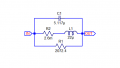
The Ltspice database doesn't have these particular components, however, the manufacturers provide the LTspice equivalent circuit to the component which is what I used
 

Thread Starter

sers000

Joined Aug 5, 2019
25
Hi,
Why are C1 and R1 added to the Inductor.?
E
Hmm i have used that component a while ago and never realised that it doesnt 100% reflect the manufacturer's equivalent circuit. In currently outside, will have a look at it when i am back. Cheers for the notice
 

Thread Starter

sers000

Joined Aug 5, 2019
25
Hey E,

I found the real component in LTspice's database:
upload_2019-8-12_20-4-14.png

Here is the schematic and its waveform with the updated component.
upload_2019-8-12_20-7-2.png

The waveforms seem too good to be true. I can't see any spikes as a result of switching.
 

ericgibbs

Joined Jan 29, 2010
18,766
hi,
Ref the spikes, you are using 'ideal' switching and not actual FETs, I would expect spikes on an actual circuit.
Looks a promising design.
E
 

Thread Starter

sers000

Joined Aug 5, 2019
25
Hey,

Yea true that makes more sense. I will implement the mosfets and see how it goes. Will update you. Cheers for the help

S
 

ericgibbs

Joined Jan 29, 2010
18,766
hi,
BTW, have you noticed the 15Apeak current rating of that inductor. ? you do not want to saturate the inductor with say 20A.
E
 

Thread Starter

sers000

Joined Aug 5, 2019
25
Greetings,

I stumbled upon Michael Engelhardt's AC analysis method to extract loop gain:
https://www.analog.com/en/technical...imulation-and-why-you-usually-don-t-need.html

Using normal ac analysis with .ac oct directive, this is the bode plot obtained:
upload_2019-10-8_21-47-33.png
, however, when using Michael Engelhardt's method, this is obtained:
upload_2019-10-8_21-51-25.png

which looks weird. I am not sure if I have implemented his method correctly. Any help here would be appreciated.

Regards,
E
 

Attachments

Last edited by a moderator:

crutschow

Joined Mar 14, 2008
34,285
was my implementation of Michael Engelhardt's method correct?
Don't know. I haven't taken the time to study it.

When I did a buck converter design, I generated a linear model (voltage gain block) for the PWM modulator and then used AC analysis to determine the loop stability margin.
The simulation is very fast and the results were quite close to the real circuit.
 
Last edited:

Thread Starter

sers000

Joined Aug 5, 2019
25
Hey again,

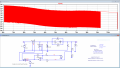
So I have been trying to minimize the noise in the circuit. I have applied a snubber consisting of a resistor and a capacitor after the switching components and the ringing effect as a result of switching has been greatly minimized. Now I am trying to minimize EMI levels to a value less than 25dBuV between 10MHz to 300MHz.What methods would you guys suggest?
Currently at the highest harmonic, its at 30 dBuV:
upload_2019-10-10_13-27-37.png
upload_2019-10-10_13-23-54.png
upload_2019-10-10_13-29-38.png
 

Attachments

Last edited:
Top