 Facebook
 Google
 GitHub
 Linkedin
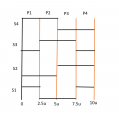
Hello, I am trying to generate the following switching pattern for a multilevel buck converter. The converter uses 4 top switches, 4 bottom switches, and 4 phases (each phase = 2.5 µs, total switching period = 10 µs). I need each top switch to follow one specific ON–OFF pattern:
How can I implement this type of switching sequence in LTspice?

- S4: ON from 0–5 µs (Phases 1 and 2), then OFF from 5–10 µs (Phases 3 and 4).
- S3: OFF from 0–2.5 µs (Phase 1), ON from 2.5–7.5 µs (Phases 2 and 3), then OFF again from 7.5–10 µs (Phase 4).
- S2: OFF from 0–5 µs (Phases 1 and 2), ON from 5–10 µs (Phases 3 and 4).
- S1: ON from 0–2.5 µs (Phase 1), OFF from 2.5–7.5 µs (Phases 2 and 3), then ON again from 7.5–10 µs (Phase 4).
How can I implement this type of switching sequence in LTspice?
Attachments
-
 13.4 KB Views: 0


