switch power supply

Thread Starter

xljin2014

Joined Nov 11, 2014
120
hi, friends,
this is a diagram of a flyback switch power supply:
Screenshot_20210804_161908.jpg

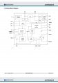
and this is the primary side ic block diagram:

Screenshot_20210804_162440.jpg

this is secondary side ic block diagram:
Screenshot_20210804_162918.jpg

I have lots of questions about the chips, and I would like to start with this, thx:
my boss told me this switch power supply uses PWM method which is generated from secondary side ic and gives back to primary side.my question is:which block of aoz7648 makes PWM signal? is it ontime generator block?as shown below:

Screenshot_20210804_164157.jpg
thank you!
 

Attachments

Delta Prime

Joined Nov 15, 2019
1,311
The first and second page of any data sheet will give you the description and the application,the pin number ,pin name and pin function that directly corresponds to the functional block diagram, is it a good idea to read the entire data sheet starting from the beginning.
 

Thread Starter

xljin2014

Joined Nov 11, 2014
120
The first and second page of any data sheet will give you the description and the application,the pin number ,pin name and pin function that directly corresponds to the functional block diagram, is it a good idea to read the entire data sheet starting from the beginning.
normally you are right. but these data sheets don't give details enough.I think I should upload data sheets.they are on chat program,and I don't know how to take them ,so I have to try.
 

Papabravo

Joined Feb 24, 2006
21,159
Yes. PWM is a periodic process with a fixed frequency. For each period of the fixed frequency clock there will be an "ON" time where a "switch" will allow current to flow in an inductor or the primary side of a transformer. Then depending on multiple criteria there will be an "OFF" time where the switch will interrupt the flow of current in the inductor or the primary of the transformer. The ratio of "ON" time to the fixed PERIOD is called the duty cycle. It is a number between 0 and 1, and can also be expressed as a percentage. It should be evident that if you have a duty cycle d, the the "OFF" time can be expressed as (1-d).

Within that framework there is one other thing that can happen. An SMPS controller can work in what is known as CCM (Continuous Conduction Mode), where there is always some current flowing in the inductor, and DCM (Discontinuous Conduction Mode), where the current in the inductor actually drops to zero during part of the "OFF" time. The use of the words continuous and discontinuous in this context does not imply that changes can take place in zero time as would be the case in mathematics when we use those terms.

I don't have a clue about what your "management" is expecting from you, but I think you are in way over your head, and I feel your pain.
 
Last edited:

Thread Starter

xljin2014

Joined Nov 11, 2014
120
Yes. PWM is a periodic process with a fixed frequency. For each period of the fixed frequency clock there will be an "ON" time where a "switch" will allow current to flow in an inductor or the primary side of a transformer. Then depending on multiple criteria there will be an "OFF" time where the switch will interrupt the flow of current in the inductor or the primary of the transformer. The ratio of "ON" time to the fixed PERIOD is called the duty cycle. It is a number between 0 and 1, and can also be expressed as a percentage. It should be evident that if you have a duty cycle d, the the "OFF" time can be expressed as (1-d).

Within that framework there is one other thing that can happen. An SMPS controller can work in what is known as CCM (Continuous Conduction Mode), where there is always some current flowing in the inductor, and DCM (Discontinuous Conduction Mode), where the current in the inductor actually drops to zero during part of the "OFF" time. The use of the words continuous and discontinuous in this context does not imply that changes can take place in zero time as would be the case in mathematics when we use those terms.

I don't have a clue about what your "management" is expecting from you, but I think you are in way over your head, and I feel your pain.
I want to know which block do the job of pwm, and how it is done(circuit)

my boss wants me to learn the data sheets and see if i can do similar.
 

Irving

Joined Jan 30, 2016
3,845
Everything you need to know is there in the data-sheets, you do have to read them fully. This is an unusual chip set, much more complex than you normally see. I do wonder about your bosses' motives here as this is not a beginners chip set and, to be fair to the data sheets, they assume some significant prior knowledge.

So here is a clue to what's going on:

The feedback (FB) pin samples the output voltage through a voltage divider and this is compared to an internal reference voltage Vref using a comparator (none of which is shown on the block diagram). If the voltage is > Vref then the OFF time is increased, if it is < Vref then the OFF time is reduced. This claims to be a constant ON time system, so the duty cycle Ton/(Ton+Toff) varies, but the frequency F = 1/(Ton+Toff) also varies so this is NOT a true PWM system where, generally, frequency is fixed and only duty cycle varies.

Now, did you understand that? If not, what didn't you understand?
 

Papabravo

Joined Feb 24, 2006
21,159
You're going to have a VERY HARD time learning anything useful from those datasheets. I've been doing this for over 30 years and I'm still a beginner. If your boss has 30 years to wait, I guess it will be fine. Here is a sample circuit from Basso, Switch-Mode Power Supplies, 2014
This is a good place to start to see if you understand what is going on.

1628101586351.png
 
Last edited:

Thread Starter

xljin2014

Joined Nov 11, 2014
120
Everything you need to know is there in the data-sheets, you do have to read them fully. This is an unusual chip set, much more complex than you normally see. I do wonder about your bosses' motives here as this is not a beginners chip set and, to be fair to the data sheets, they assume some significant prior knowledge.

So here is a clue to what's going on:

The feedback (FB) pin samples the output voltage through a voltage divider and this is compared to an internal reference voltage Vref using a comparator (none of which is shown on the block diagram). If the voltage is > Vref then the OFF time is increased, if it is < Vref then the OFF time is reduced. This claims to be a constant ON time system, so the duty cycle Ton/(Ton+Toff) varies, but the frequency F = 1/(Ton+Toff) also varies so this is NOT a true PWM system where, generally, frequency is fixed and only duty cycle varies.

Now, did you understand that? If not, what didn't you understand?
so I'm right that the on time generator does the job of PWM ?
 

Papabravo

Joined Feb 24, 2006
21,159
Yes you are correct in your last two posts. I have not looked at the whole datasheet, but I will if you ask me. In my experience you get a block diagram and that is about it. with the simulation that I posted you can see that there are two control loops. One responds to the output voltage, and the other responds to the magnitude of the current peak during the on time with slope compensation. This is a simple buck converter, not a flyback, but the principles of closing the loop are similar.

Do you need an explanation of the control scheme that I posted?
 

Thread Starter

xljin2014

Joined Nov 11, 2014
120
You're going to have a VERY HARD time learning anything useful from those datasheets. I've been doing this for over 30 years and I'm still a beginner. If your boss has 30 years to wait, I guess it will be fine. Here is a sample circuit from Basso, Switch-Mode Power Supplies, 2014
This is a good place to start to see if you understand what is going on.

View attachment 245059
I don't quite understand about the circuits, can you give me some clues?
 

Thread Starter

xljin2014

Joined Nov 11, 2014
120
Yes you are correct in your last two posts. I have not looked at the whole datasheet, but I will if you ask me. In my experience you get a block diagram and that is about it. with the simulation that I posted you can see that there are two control loops. One responds to the output voltage, and the other responds to the magnitude of the current peak during the on time with slope compensation. This is a simple buck converter, not a flyback, but the principles of closing the loop are similar.

Do you need an explanation of the control scheme that I posted?
I don't see you posted any scheme, but I would like to have it and your explanation, ty.
 

Papabravo

Joined Feb 24, 2006
21,159
I don't quite understand about the circuits, can you give me some clues?
In post #8, there is an image of a simulation. Can you see that image?

The power circuit including V1, S1, D1, L1, C1, and R1 is a buck regulator with a 10 VDC input and a 5 VDC output. This example is chosen because it sets the nominal duty cycle at 50% which can be a problem for buck converters without slope compensation. The switching frequency is 10 kHz, defined by the "Tclock" parameter of 100 μsec. Switch S1 closes at the beginning of every 100 μsec interval and it opens whenever the voltage gets to large or the peak current is exceeded. When the switch opens the voltage at the junction of the diode and the inductor goes negative and the diode conducts allowing the current to circulate from the capacitor, through the diode, through the inductor and into the load. then the cycle stars over again during the next 100 μsec period.

The controller consists of several things going on simultaneously. We can work from the output voltage forward to the RS flip-flop or we can work backward from the RS flip-flop to the output voltage. You decide which way makes more sense.
 

Irving

Joined Jan 30, 2016
3,845
so I'm right that the on time generator does the job of PWM ?
and the data sheet doesn't tell how(circuit)?
That's correct. But this isn't uncommon; the data-sheet is there to give you information to use the device, not to teach you how to design one. It assumes you have a good understanding of the general principles.

Papabravo has posted a simple example and simulation of a buck converter and it's control loop. While not directly comparable to this chip-set he's trying to establish your existing level of knowledge as did I in post #7.

If you want more help it would be helpful if you respond to those posts.
 

Thread Starter

xljin2014

Joined Nov 11, 2014
120
Everything you need to know is there in the data-sheets, you do have to read them fully. This is an unusual chip set, much more complex than you normally see. I do wonder about your bosses' motives here as this is not a beginners chip set and, to be fair to the data sheets, they assume some significant prior knowledge.

So here is a clue to what's going on:

The feedback (FB) pin samples the output voltage through a voltage divider and this is compared to an internal reference voltage Vref using a comparator (none of which is shown on the block diagram). If the voltage is > Vref then the OFF time is increased, if it is < Vref then the OFF time is reduced. This claims to be a constant ON time system, so the duty cycle Ton/(Ton+Toff) varies, but the frequency F = 1/(Ton+Toff) also varies so this is NOT a true PWM system where, generally, frequency is fixed and only duty cycle varies.

Now, did you understand that? If not, what didn't you understand?
thx for your great reply. sorry I was busy yesterday and didn't reply on time.

I looked the chip diagrams and got some ideas.and now I need to know inside circuits.but now I want to ask you a question, it's about transmitter and receiver block.I think the PWM signal is produced from aoz7648 and send to aoz7635,so it should be transmitter for 7648 and receiver for 7635,but the diagrams show both are transmitter and receiver. which means signals go forth and back, I don't understand this.

maybe I should go to ic design groop, lol.

thx again! and greetings!
 

Irving

Joined Jan 30, 2016
3,845
I think the PWM signal is produced from aoz7648 and send to aoz7635,so it should be transmitter for 7648 and receiver for 7635,but the diagrams show both are transmitter and receiver. which means signals go forth and back, I don't understand this.
That's correct and I am not sure if its two way or one way transmission. The pin names suggest one way but, as you saw, the boxes in each block diagram suggest 2-way. The text of both data sheets suggest 1-way which makes sense to me as that is all that's needed.

I think whoever drew the pictures was just a bit lazy!
 

Papabravo

Joined Feb 24, 2006
21,159
thx for your great reply. sorry I was busy yesterday and didn't reply on time.

I looked the chip diagrams and got some ideas.and now I need to know inside circuits.but now I want to ask you a question, it's about transmitter and receiver block.I think the PWM signal is produced from aoz7648 and send to aoz7635,so it should be transmitter for 7648 and receiver for 7635,but the diagrams show both are transmitter and receiver. which means signals go forth and back, I don't understand this.

maybe I should go to ic design groop, lol.

thx again! and greetings!
The blocks in the block diagram say "Transmitter & Receiver", but the signal lines are labeled in such a way that communication in one direction only is implied. Why not get an FAE on the phone and just ask them. Is there some reason why you haven't done that?
 

Thread Starter

xljin2014

Joined Nov 11, 2014
120
Everything you need to know is there in the data-sheets, you do have to read them fully. This is an unusual chip set, much more complex than you normally see. I do wonder about your bosses' motives here as this is not a beginners chip set and, to be fair to the data sheets, they assume some significant prior knowledge.

So here is a clue to what's going on:

The feedback (FB) pin samples the output voltage through a voltage divider and this is compared to an internal reference voltage Vref using a comparator (none of which is shown on the block diagram). If the voltage is > Vref then the OFF time is increased, if it is < Vref then the OFF time is reduced. This claims to be a constant ON time system, so the duty cycle Ton/(Ton+Toff) varies, but the frequency F = 1/(Ton+Toff) also varies so this is NOT a true PWM system where, generally, frequency is fixed and only duty cycle varies.

Now, did you understand that? If not, what didn't you understand?
thx for your great reply. sorry I was busy yesterday and didn't reply on time.

I looked the chip diagrams and got some ideas.and now I need to know inside circuits.but now I want to ask you a question, it's about transmitter and receiver block.I think the PWM signal is produced from aoz7648 and send to aoz7635,so it should be transmitter for 7648 and receiver for 7635,but the diagrams show both are transmitter and receiver. which means signals go forth and back, I don't understand this.

maybe I should go to ic design groop, lol.

thx again! and greetings
That's correct and I am not sure if its two way or one way transmission. The pin names suggest one way but, as you saw, the boxes in each block diagram suggest 2-way. The text of both data sheets suggest 1-way which makes sense to me as that is all that's needed.

I think whoever drew the pictures was just a bit lazy!
oh,I'm always so stupid to trust they are all correct.

I may go to ic design block, would you help me there?

thx again.
 
Top