Maybe, but an LVC1G14 does not have two inputs. It only has 1 input, so I would keep searching. It is true that pin 1 is a no connect for that package so it is still possible, just unusual for the layout person to do that.
I have doubts about the drawing supplied.
If the output is generated from PB6 from an STM32F103 why would they need to buffer or invert the logic signal?
If the purpose is to drive the emitter in an opto-isolator, why the need for the 180Ω resistor to GND?
The emitter of NEC9587 forward voltage is 1.65V typical, 1.8V max. Hence it could be have been driven directly by the STM32F103.
The 390Ω resistor serves no purpose but to waste power.
There are many SN74LVC1Gxx gates that match that pinout, for example, SN74LVC1G00.
Vcc on pin-5 would need +V supply.
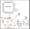
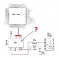
I have doubts about the drawing supplied. View attachment 264821
If the output is generated from PB6 from an STM32F103 why would they need to buffer or invert the logic signal?
If the purpose is to drive the emitter in an opto-isolator, why the need for the 180Ω resistor to GND?
The emitter of NEC9587 forward voltage is 1.65V typical, 1.8V max. Hence it could be have been driven directly by the STM32F103.
The 390Ω resistor serves no purpose but to waste power.
There are many SN74LVC1Gxx gates that match that pinout, for example, SN74LVC1G00.
Vcc on pin-5 would need +V supply.
If the output is generated from PB6 from an STM32F103 why would they need to buffer or invert the logic signal?
If the purpose is to drive the emitter in an opto-isolator, why the need for the 180Ω resistor to GND?
The emitter of NEC9587 forward voltage is 1.65V typical, 1.8V max. Hence it could be have been driven directly by the STM32F103.
The 390Ω resistor serves no purpose but to waste power.
 Facebook
 Google
 GitHub
 Linkedin
 94.1 KB Views: 21