Slayer Exciter Circuit- analysis

Thread Starter

davidcoll

Joined Apr 30, 2018
16
Hi,
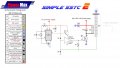
im a physics student and im doing a project on Slayer Excitor- a resonance transformer, for a lab course in the university. i attached the cirucit file that i found online, design be PoweMax.
my first question: i know that the mosfet Q1 is oscillated with a 10% duty cycle square wave with frequency around 60 hz from the 555, what is the output signal and frequency in L2, and how can i calculate it?

what is the role of C4 and C1 capacitors in the circuit?

and what is the role of D2 and D3 diodes?

and last question: L2 output an increaed voltage but have large inner resistance. how this device efficient?

https://www.instructables.com/id/Easy-SSTC-Slayer-Exciter-On-Steroids/


Thanks.
 

Attachments

ebp

Joined Feb 8, 2018
2,332
The diodes:
The DS0026 (a very old part, originally a clock driver for dynamic RAM) has either deliberately-made or "parasitic" diodes from the input to the power supply pins. These diodes will conduct if the input voltage is greater than the positive power supply pin voltage or less than the negative (common, or "ground") pin voltage. If the current is not limited the internal diodes can be destroyed. One way to protect the input is to use bigger diodes externally. The bigger diodes can conduct much more current safely and usually conduct at a voltage low enough that the internal diodes only conduct a little. If you look at specifications in detail, just adding the external diodes often isn't adequate to assure meeting the spec's, but in practice it usually is.

Because the circuit is a transformer and the "bottom" of the output winding goes back to the input of the gate driver in order to make the circuit oscillate, there is a chance (certainty, actually) that without the external diodes to conduct current the internal diodes would conduct too much and be damaged. D2 and D3 protect the input from excessive voltage and excessive current.

The way the 0026 is designed is such that to make the input logic HIGH you have to make current flow into the input ("into" here referring to "conventional current" which is considered to flow from positive to negative). If the input is open-circuit, it behaves like it is at logic LOW. With many gate drivers it would be necessary to use a resistor to be sure that the input logic level was correct if nothing else was driving the input. It the driver input were HIGH if left open-circuit, this circuit would never start up.

C4
When the MOSFET is ON, the current though it must be very high. Normally you would expect the power supply to directly deliver the required current, but I suspect the circuit designer used a power supply that can only deliver the average value of the required current and not the short, very high current peaks. The large capacitor just serves as a reservoir for energy - it delivers most of the high peak current and the main power supply only "sees" the average current. C4 needs to be close to the rest of the circuit so the resistance and inductance of the connections is small.

C1 - this one you need to figure out for yourself. It is a key component in the operation of the circuit and you actually used a word that describes why it is there in your first sentence.
 

Thread Starter

davidcoll

Joined Apr 30, 2018
16
The diodes:
The DS0026 (a very old part, originally a clock driver for dynamic RAM) has either deliberately-made or "parasitic" diodes from the input to the power supply pins. These diodes will conduct if the input voltage is greater than the positive power supply pin voltage or less than the negative (common, or "ground") pin voltage. If the current is not limited the internal diodes can be destroyed. One way to protect the input is to use bigger diodes externally. The bigger diodes can conduct much more current safely and usually conduct at a voltage low enough that the internal diodes only conduct a little. If you look at specifications in detail, just adding the external diodes often isn't adequate to assure meeting the spec's, but in practice it usually is.

Because the circuit is a transformer and the "bottom" of the output winding goes back to the input of the gate driver in order to make the circuit oscillate, there is a chance (certainty, actually) that without the external diodes to conduct current the internal diodes would conduct too much and be damaged. D2 and D3 protect the input from excessive voltage and excessive current.

The way the 0026 is designed is such that to make the input logic HIGH you have to make current flow into the input ("into" here referring to "conventional current" which is considered to flow from positive to negative). If the input is open-circuit, it behaves like it is at logic LOW. With many gate drivers it would be necessary to use a resistor to be sure that the input logic level was correct if nothing else was driving the input. It the driver input were HIGH if left open-circuit, this circuit would never start up.

C4
When the MOSFET is ON, the current though it must be very high. Normally you would expect the power supply to directly deliver the required current, but I suspect the circuit designer used a power supply that can only deliver the average value of the required current and not the short, very high current peaks. The large capacitor just serves as a reservoir for energy - it delivers most of the high peak current and the main power supply only "sees" the average current. C4 needs to be close to the rest of the circuit so the resistance and inductance of the connections is small.

C1 - this one you need to figure out for yourself. It is a key component in the operation of the circuit and you actually used a word that describes why it is there in your first sentence.
Sir, thank you so much for your answer, and help!

I think i got it. when the capacitor is fully charged and then discharge, its oscillate with the inductor, and EXP decrease. because of that there is an offset square wave, to charge the capacitor and then let him discharge when the voltage input is zero. all this done by the mosfet who acts like a switch.
and last question: its a sine wave in L1, does L2 output a derivative signal? a cosine?

again,
Thank you.
 
Last edited:
Top