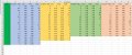
I have attached a picture below showing the results i have gotten. On a side note, I noticed in LTspice, to get Vout = 9V, my pot would have to be 33K Ohms. However during the test, I'm getting 9V at 45K. I have included the pot setting next to the Vout in the picture.
Hi Johnny,
If you could post a text file of the results, I can import them into my spreadsheet, saves me a lot of typing.
E EDIT:
A quick look at the 4 groups of results, show a Vout fall off occurring around the 400mA output current mark.
12V 4.8W
9V 3.6W
5V 2.0W
3V 1.0W
I am impressed and horrified that you are doing this on a solderless breadboard.
I would NEVER attempt evaluating any SMPS design on those things.
Even on a PCB, I have had issues with stability, noise and voltage drops due to poor layout.
500 Khz is well into RF, you need to lay these out like RF circuits, solderless breadboards are a disaster at RF.
Hi Johnny,
If you could post a text file of the results, I can import them into my spreadsheet, saves me a lot of typing.
E EDIT:
A quick look at the 4 groups of results, show a Vout fall off occurring around the 400mA output current mark.
12V 4.8W
9V 3.6W
5V 2.0W
3V 1.0W
Sorry about that, I'll keep that in mind. The results are fine right? I don't really know the standards. and also, what other tests should i do? I was advised to use a spectrum analyzer but i am not quite sure what to look for.
I am impressed and horrified that you are doing this on a solderless breadboard.
I would NEVER attempt evaluating any SMPS design on those things.
Even on a PCB, I have had issues with stability, noise and voltage drops due to poor layout.
500 Khz is well into RF, you need to lay these out like RF circuits, solderless breadboards are a disaster at RF.
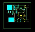
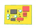
I have updated my PCB design, taking into account the loop considerations and design layout provided in the datasheet. This is how it looks. I appreciate any feedback.
The track width is 1.3mm , except for the feedback and Vcc track , which was reduced to 0.5mm and 0.8mm to meet the design rule check requirements.
1) I have added a copper area on my IC's ground tab to act both as a GND and heatsync, is that a good idea?
Ground is your friend, it's the reference for the entire circuit, make it as low impedance as possible.
Flood it out to the edges, make it fat and wide- it's called the GROUND PLANE for a reason.
Remember, you already paid for the copper on the board, use it to make solve your design problems.
Look at some professional boards, note how they tend to leave a lot of copper, it's being used!
Think about where the heavy current flows, make those traces as short and fat as possible.
It's the mark of a neophyte PCB designer to have skimpy traces of all the same width.
Really badass designers make "shapes" more than "traces"- these shapes connect elements with the lowest possible resistance.
hi J,
There are number points wrong with the PCB track.
I will post back, shortly.
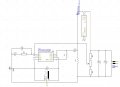
It would help in the mean time, if you added the actual circuit diagram to post 72
E
hi J,
There are number points wrong with the PCB track.
I will post back, shortly.
It would help in the mean time, if you added the actual circuit diagram to post 72
E
hi J,
Sorry, but I would not accept that tracking and layout as being good enough for etching.
If the thru vias are not plated, how do you intend top soldering the electrolytics.
Do you plan to etch and drill the PCB yourself.?
E
EDIT:
Also soldering the trim Pot and other top side components, will be a problem.
hi J,
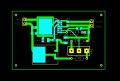
This marked up PCB image should give you a better idea of what changes are required, check it thru, ask if you see any problems.
The non component side N/C is your Common/0V plane, once you have laid and isolated any non 0v tracks on the N/C side, you can flood fill the remainder with copper.
This is a Draft layout, so double check it.
Don't forget to add PCB fixing holes at the corners.
E
hi J,
This marked up PCB image should give you a better idea of what changes are required, check it thru, ask if you see any problems.
The non component side N/C is your Common/0V plane, once you have laid and isolated any non 0v tracks on the N/C side, you can flood fill the remainder with copper.
This is a Draft layout, so double check it.
Don't forget to add PCB fixing holes at the corners.
E
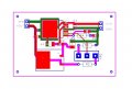
I hope this is what you meant. I have the output capacitors and the ground tab connected through copper pour. I tried to keep the Vsw, output diode and capacitor as close as possible, and moved the inductors away from the compensation and feedback.
I have yet to change the trace width but please take a look.
Thanks
J
EDIT: By N/C side, did you mean i should place those components on the other side of the board?
hi J,
I assume that the Blue track is on the component side of the PCB and the Green track is on the non component side.?
Which means all the through hole components can soldering at the non comp side.?
The tracks widths should be increased, where possible.
hi J,
I assume that the Blue track is on the component side of the PCB and the Green track is on the non component side.?
Which means all the through hole components can soldering at the non comp side.?
The tracks widths should be increased, where possible.
Hi Eric,
Oh yes, all through holes will be soldered from the bottom layer of the PCB. ( All components are placed on top layer )
I plan to change the width of the traces if the layout checks out.
hi,
It is looking close to being finished.
Check what the switcher datasheet says about linkingthe SS pin
The component drill thru hole should be 1mm dia
For the switcher and surface mount components, how do you intend making the track contact from non side to comp side.??? Corrected the SS pin link.
E EDIT: the usual way is a pad on both sides, with a1mm dia hole, solder in a copper wire link thru.
When doing PCB design layout you should have 3 dimensional model in your mind.
 Facebook
 Google
 GitHub
 Linkedin