That's because the character pitch used in the 'editor' differs from that of posted text --- No problem!
Please identify the position of the positive probe while taking each of the above readings...
Very best regards
HP
PS what does "K.Reg" mean?![]()
That's because the character pitch used in the 'editor' differs from that of posted text --- No problem!
Please identify the position of the positive probe while taking each of the above readings...
Very best regards
HP
PS what does "K.Reg" mean?![]()
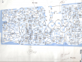
Yes, please post a copy -- all I have is the schematic...I guess you have it at yr disposition? if not i'll copy it.
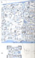
Perfect! -- Thank you!Cannot copy it in 1 piece...to large. Requested info was on components at left 1/3 /top of first (left) half.
View attachment 99099
View attachment 99100
No problem; Fantastic that you study the problem!Perfect! -- Thank you!
I apologize that won't have much time to participate on the fora today -- However I will get back with you tomorrow!
HP
Indeed. "top", "below" I mentioned etc was referenced to the schematic I I 'll take care to add it next time.@patpin
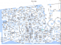
In the interest of reduction of liability to error, as well as optimization of my time so as to best assist your troubleshooting efforts - let's adopt a protocol such that citation of a component's position/orientation is with sole referance to its symbol upon the schematic diagram (below)
Please know, for instance, that I've just spent 30 minutes correlating positions on the wiring diagram with those on the schematic -- time that would have been much better invested analyzing the readings, etc...
So, based upon the wiring diagram and post #182
The positive indicator probe was connected to:
-The bottom of R64 as shown on the schematic
-The top of R65 as shown on the schematic
-The bottom of D55 as shown on the schematic
Please verify the above
Best regards
HP
PS -- For your convenience, you may wish to consider printing a hard-copy of the schematic for ready reference
![]()
Please make all references with respect to the schematic (i.e. Top, Bottom, Left, Right)Indeed. "top", "below" I mentioned etc was referenced to the schematic I I 'll take care to add it next time.
I checked the PCB layout versus diagram, which indeed takes a lot of time ↑Please identify the position of the positive probe while taking each of the above readings...
I have to thank you!!@patpin
I apologize for my scarcity as of late -- I'll try to get back to you soon! (Tomorrow or this weekend at latest) -- Many thanks for your work/observations and patience!!!
Very best regards
HP![]()
Thank you for your patience!I have to thank you!!![]()
Home is @ ≈47° N latitude --- Though I tend to spend a good deal of time at ≈45° N Lat and even more at ≈49°NOn which latitude are U situated?
waw ... must be 'cool' outhereThank you for your patience!
Home is @ ≈47° N latitude --- Though I tend to spend a good deal of time at ≈45° N Lat and even more at ≈49°N
Best regards
HP![]()
Being, as I am, at the center of a large continent, what can I say? - Too hot in summer! - Too cold in winter! --- Sadly, comfort is seldom to be found among the splendors of 'the great outdoors'waw ... must be 'cool' outhere
Thanks for info. I 'll check this WE. Whats the expected effect of freezing. Worse or better?Hey @patpin
Here's something for you to try in the meantime:
Inasmuch as many of the symptoms are consistent with a 'bad connection' (e.g. a cracked trace at a solder pad) try prodding the the board while observing the display -- The circuitry associated with TR26 and TR31 with special emphasis upon areas about R69, R68, etc... is especially suspect... But please 'explore' all circuitry associated with TR33 and TR37 as well...
Note: It goes without saying that the 'prod' must be fashioned an insulating material (as, for instance, a 'Biro' with tip and ink tube removed -- But under no circumstances a pencil - as graphite is an electrical conductor!)
Please don't be discouraged if the above procedure produces nil results -- I'm prepared to 'buckle down' on this starting Monday!
Best regards
HP
PS -- FWIW Another 'trick' occasionally effective in the location of defective components/connections is careful application of 'freeze spray' to suspect components/areas of the PC Board --- (Note that fluorocarbon 'dusting spray' will also work however the can must be inverted to dispense the liquid) -- If you choose to try this, you are strongly advised to obtain a 'denaturant' (a.k.a. 'bittering agent') free product -- One may often find the unadulterated product at retailers specializing in photography supplies...