Schematic Review: MAX30003 and nRF52840 (XIAO)

Thread Starter

Nammm

Joined Mar 9, 2026
16
Hi everyone,

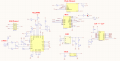
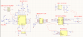
I am working on a wearable ECG monitoring device and would appreciate some feedback on my schematic before I proceed to the PCB layout.

Project Overview:

  • MCU: Seeed Studio XIAO nRF52840.
  • Analog Front-End: MAX30003 (Biopotential AFE).
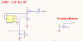
  • Power: The system uses the 3.3V rail from the XIAO, which is stepped down to 1.8V to power the MAX30003.
  • Storage: W25Q128 Flash Memory for data logging.
  • Clock: External 32.768kHz oscillator (SiT1533) for the MAX30003.
Is there anything wrong in my schematic and how can I improve it. It makes me so nervous. Thank you all.

1777527930102.png
 

Attachments

Last edited:

Sensacell

Joined Jun 19, 2012
3,770
1) Ground symbols always vertical- NEVER sideways or upside-down.
2) Just using NET labels might make a PCB design program happy- but it does nothing for schematic readability.

The job of a schematic is to make the design understandable, make this a priority.


Arrange the drawing so the general signal flow is top-to-bottom, left-to-right.
Draw the connections so the eye can see and follow the signal flow, rather than forcing a reader to hunt for matching signal names.
Use net labels where it makes sense- but not as primary connectivity.

When I see a schematic like this- I don't feel like reading it, it's too much work, so I skip it- and that would be your loss.
 

Irving

Joined Jan 30, 2016
5,010
No need for level translator, digital inputs (SDI, SCLK, FCLK, CSB) & outputs (SDO, INTB, INT2B) on the MAX30003 are 3.3v tolerant, just connect OVDD to 3.3v not 1.8v.
 

Rf300

Joined Apr 18, 2025
73
You need at least a level shifter for the outputs of MAX30003. With a 1.8 V supply you will never get the min. HIGH input voltage of 2.0 V for a 3.3 V CMOS-Input. The cheap and nasty solution would be a pull-up of 4.7 kOhm to 3.3 V, the correct solution is the level shifter.
 

Thread Starter

Nammm

Joined Mar 9, 2026
16
You need at least a level shifter for the outputs of MAX30003. With a 1.8 V supply you will never get the min. HIGH input voltage of 2.0 V for a 3.3 V CMOS-Input. The cheap and nasty solution would be a pull-up of 4.7 kOhm to 3.3 V, the correct solution is the level shifter.
that right, so I used TXS0108E so it can convert 1.8v to 3.3v for MCU understanding. I wonder is there any logic wrong in my routing wire . Thanks
 

Thread Starter

Nammm

Joined Mar 9, 2026
16
No need for level translator, digital inputs (SDI, SCLK, FCLK, CSB) & outputs (SDO, INTB, INT2B) on the MAX30003 are 3.3v tolerant, just connect OVDD to 3.3v not 1.8v.
Sure but for personal reasons, I have to use 1.8v. Thanks for great opinion, beside I wonder is there any logic wrong in my routing wire
 

Irving

Joined Jan 30, 2016
5,010
You need at least a level shifter for the outputs of MAX30003. With a 1.8 V supply you will never get the min. HIGH input voltage of 2.0 V for a 3.3 V CMOS-Input. The cheap and nasty solution would be a pull-up of 4.7 kOhm to 3.3 V, the correct solution is the level shifter.
I beg to differ, the correct engineering solution is to power the I/O circuits from 3.3v as per the datasheet, unless you know of a specific and valid reason not to do so? I'll admit I've never used the MAX30003, but I didn't find any documented issues regarding using 3.3v to power OVDD.

Sure but for personal reasons, I have to use 1.8v. Thanks for great opinion, beside I wonder is there any logic wrong in my routing wire
'personal reasons'? Sorry, use of the translator offends my personal belief that, unless there are good engineering reasons not to do, minimising chip count and connections enhances reliability and minimises costs, assembly time, etc. That's not an opinion, that's engineering fact. But it's your board, you do what you like.
 

Thread Starter

Nammm

Joined Mar 9, 2026
16
I beg to differ, the correct engineering solution is to power the I/O circuits from 3.3v as per the datasheet, unless you know of a specific and valid reason not to do so? I'll admit I've never used the MAX30003, but I didn't find any documented issues regarding using 3.3v to power OVDD.


'personal reasons'? Sorry, use of the translator offends my personal belief that, unless there are good engineering reasons not to do, minimising chip count and connections enhances reliability and minimises costs, assembly time, etc. That's not an opinion, that's engineering fact. But it's your board, you do what you like.
sorry for the poor phrasing. I chose 1.8V for OVDD to maximize battery life for this compact wearable (LIR2450) and to minimize switching noise/EMI on the sensitive ECG traces. Lower voltage swings mean less crosstalk into the AFE. thanks
 

Irving

Joined Jan 30, 2016
5,010
sorry for the poor phrasing. I chose 1.8V for OVDD to maximize battery life for this compact wearable (LIR2450) and to minimize switching noise/EMI on the sensitive ECG traces. Lower voltage swings mean less crosstalk into the AFE. thanks
Have you actually done a power budget analysis for this section? If so, can you share it, or is this just gut feel?

For a start, the Iovdd @1.65v/4MHz is 0.2uA typical rising to a max of 1.6uA at 3.6v/4MHz. The quiescent (non-switching) total supply current of the TXS0108E is typically 3uA, so by adding it you've already increased the potential current draw from a max of 1.6uA to a typical of 3.2uA! And that doesn't include the switching losses on both sides of the translator... What is your proposed SPI clock speed?

Good board layout, careful guarding around the AFE and careful routing of SPI lines will do far more for x-talk than reducing the voltage swing on the I/O.

Anyway, all of that is swamped by the nRF52840. We're using a Sense module to read 16 passive resistive sensors via an external mux (2.5mA) together with a 128Mbit WinBond NOR flash and a 170mA 3.7v LiPo pouch, all squeezed into a 30 x 26 x 9mm package. At 200Hz, 16ch x 10 bit sampling and 1Mbps transmission over BLE5 we get about 5h run time on a duty cycle of 30% (1.5mS acquisition & transmission per 5mS).
 

Thread Starter

Nammm

Joined Mar 9, 2026
16
thanks Irving, your suggestion really amazed me, ill go with 3.3V for the MAX30003 and remove the signal conversion block entirely. This is my second post in ACC, but you always give such helpful advice
 

Irving

Joined Jan 30, 2016
5,010
thanks Irving, your suggestion really amazed me, ill go with 3.3V for the MAX30003 and remove the signal conversion block entirely. This is my second post in ACC, but you always give such helpful advice
#1 requirement for any wearable tech is both static and dynamic power budget analysis. It isn't always very easy and datasheets rarely give enough info. Which is why I asked about your proposed SPI clock speed - switching losses are directly proportional to clock speed.

Thank you, I do my best. It's a great community here and we all learn from each other.
 

Thread Starter

Nammm

Joined Mar 9, 2026
16
#1 requirement for any wearable tech is both static and dynamic power budget analysis. It isn't always very easy and datasheets rarely give enough info. Which is why I asked about your proposed SPI clock speed - switching losses are directly proportional to clock speed.

Thank you, I do my best. It's a great community here and we all learn from each other.
Hi Irving, could you do a final check on this for the last one before I move on to the PCB layout. Thank you so much
1777527649845.png
 
Top