Schematic Reconstruction of a 12V,1A SMPS Charger

Thread Starter

khatus

Joined Jul 2, 2018
115
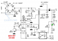
Hello guys, I have tried to reverse engineer a 12V, 1A SMPS charger circuit and draw its schematic. My question is: is this circuit technically correct? Could there be any mistakes in it? I was specifically inspired by the DiodeGoneWild YouTube channel for this project.

12V_1A_smps.jpg
 

Irving

Joined Jan 30, 2016
5,066
Not sure about the PNP/NPN transistor pair - some sort of relaxation oscillator, but otherwise it's a common setup. But if you were thinking to build another one, don't, as there are simpler and mostly cheaper options than this ancient design.
 

MisterBill2

Joined Jan 23, 2018
27,315
The circuit may be correct, I don't have the original to compare. There are some parts a bit hard to follow, but most of the arrangement is OK.
The line ti that 1KV capacitor that cuts thru the transformer should not be placed there. Other than that the drawing is OK.
 

MisterBill2

Joined Jan 23, 2018
27,315
That circuit line passing thru the transformer symbol should not pass thru the symbol, because it splits the transformer into two separate inductors, totally changing the meaning. As for the actual circuit being shown, presenting the capacitor is OK, except for the confusion it causes.
BTW, the transistor part of the opto isolator, as I see it in this image, is not serving any valid purpose.
 

MisterBill2

Joined Jan 23, 2018
27,315
THAT flaw hit me before I started to evaluate the circuit. Certainly the sections of the opto isolator are reversed, the LED should be towards the power supply OUTPUT end, and the transistor side should connect to the 8050/8550 transistors. The transformer was a big distraction.
I should clarify that I have been reading circuits for MANY years, so they are my first language. so the transformer stood out! I have not decided if the system will actually oscillate,but with the opto correctly connected it has a chance.
 

Irving

Joined Jan 30, 2016
5,066
I agree with @MisterBill2 , the LED of the opto should be in the secondary side, and the transistor on the primary side. I also missed that on first glance!

The cathode (bar) of the LED to the zener/1Mohm junction and the anode to +12v rail. When the voltage across the zener reaches 11v the it starts to clamp establishing an 11v node at its cathode. As the output voltage rises above about 12v the opto LED turns on shutting down the relaxation oscillator thus regulating the output. I don't think overall runaway oscillation is possible. On the primary side, the opto transistor emitter goes to the base of the NPN.

The PNP/NPN pair is a clamp, like a mini-thyristor. When either transistor starts to turn on there is an avalanche effect and each turns the other on hard and it remains that way until either the current through the pair falls to zero or the base of the NPN is pulled -ve.

When power is initally applied the clamp is off. The rising voltage turns the MOSFET on and current flows through the primary winding building up magnetic flux in the core. When the current reaches a certain level the voltage across the 1.2ohm resistor exceeds 0.6v and actives the clamp turning the MOSFET off. The collapsing magnetic field induces voltage in the secondary windings, producing output power and an auxiliary supply current through the 1k resistor & 15nF capacitor holds the clamp on. That current drains away, the clamp turns off, the MOSFET turns back on and the cycle repeats.

During the MOSFET on time, induced current in the aux winding charges the 4.7u capacitor, the zener acting as a rectifier. If the opto transistor is on because the output is high that aux voltage turns the clamp on killing oscillation until the output voltage drops low enough to turn the clamp off and allow oscillation to resume.
 

MisterBill2

Joined Jan 23, 2018
27,315
OK, I have neglected to comment on the effect of that "AUX" winding, which is also part of the transformer, and needs to be included in the transformer symbol somehow.

Consider that the main purpose of a schematic circuit drawing is to convey information about the circuit, the actual details ARE IMPORTANT! The other purpose of the drawing is to allow the designer to keep their thoughts organized while creating the complete system. That is also important.
 

ronsimpson

Joined Oct 7, 2019
4,661
I have too much experience with this "design" and its brothers. Somewhere today there is an engineer in a small company trying to make this work. After months he got several to work but when they went into production they stopped. AND/OR When they changed transformer vendors, it stopped working. AND/OR When the room temperature changed it stopped working. This engineer copied the idea from a Chinese company, that copied it from a Korien company that copied it from a Japan company. Each time some unlucky engineer had to change every RC in the circuit. Every time the transformer design was a very large struggle. The design depends on the transformer leakage inductance, resonant frequency and saturation point. None of this is in the schematic. There is too much black magic in this.
 

schmitt trigger

Joined Jul 12, 2010
2,056
Having worked for a large power supply manufacturer, I agree 100%, no 200% with Ron’s statement.
These self-oscillating designs were viable in the late 1970s, when no off-line SMPS IC controllers were available. Nowadays there are many low cost and simple devices from many manufacturers.
 

MisterBill2

Joined Jan 23, 2018
27,315
Given that RS and also ST are right, and considering the relative complexity of the proposed circuit, I have a suggestion::
Forget this circuit, unless the intent is to learn from doing the analysis, and copy a much simpler circuit published in 1963 by the General Electric COMPANY, for a functionally similar performance charger. The huge difference is in the transformer, which i the original circuit was able to provide at least ten amps of charging current.
 

Irving

Joined Jan 30, 2016
5,066
OK, I have neglected to comment on the effect of that "AUX" winding, which is also part of the transformer, and needs to be included in the transformer symbol somehow.

Consider that the main purpose of a schematic circuit drawing is to convey information about the circuit, the actual details ARE IMPORTANT! The other purpose of the drawing is to allow the designer to keep their thoughts organized while creating the complete system. That is also important.
Ok, now I'm going to disagree with you on two points and the first is your need for the transformer to be one symbol. We don't, often, do that with the optocoupler, or relay contacts and coil, or multi-component digital devices, so why mandate it with the transformer? I've looked at enough manufacturer's datasheets to know there are at least two or three windings on the transformer. Yes, it would be nice to have a transformer detail grid but probably one never existed. I'm happy with the coils being separate, though it would be great to have component designations ie R1, R2, C1, C2, etc and therefore T1:N1,T1:N2 and T1:N3 to show they were related.

Also, step back and consider where the diagram came from; its a reverse engineer of an actual PCB by someone who isn't a professional, so kudos they got this far. I've never posted a diagram drawn by hand of anything; it's always KICad, Onshape/SolidWorks, etc., even, sadly, LTSpice for circuit simulation though the quality of the schematic drawing annoys me alongside the quality of the simulation results (and it bugs me that the Spice simulation tools in KICad aren't up to scratch; though I hear that KICad #10 goes along way to address this in part.) As a professional, anything less goes against the grain, even for hobby stuff, but I also recognise that not everybody has access or capability with those tools and I make allowances.
 

MisterBill2

Joined Jan 23, 2018
27,315
Did you notice that the transformer was the only item that I commented about?? Other than that, My post #3 was complementary. and yes, I was aware that it was a "reverse engineering" effort. I have done quite a fewof those. And mostly the "first draft" gets abandoned well prior to completion, because it is excessivey hard to follow.
 
Top