Facebook
 Google
 GitHub
 Linkedin
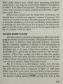
Recently deciding to complete my 1987 project (!!) from the 1979 book “How to Build Your Own Self programming Robot” (by David L Heiserman) that I started whilst at college I would like to confirm a few possible circuit errors that I’ve noted.
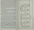
From Schematic 11.2(attached);
Memory Address lines MA0 - MA3 pass through the 74LS367 buffer/driver (IC Z121) on the lower 4 (of 6) gates,whilst MA4 & 5 pass through on the upper 2 gates.
MA6 & MA7 pass through on the bottom 74LS367 (IC Z122), but the input-output pins 11/12 & 13/14 appear crossed.
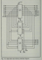
The same error also appears on schematic 11-3 for the High-order memory bits MA14 and MA15. Scrutinizing even further it looks like the data lines MD4-MD7 (on Z1191) are also crossed as these connect to the Data-In pins of the RAM chips*. The same error being seen back on schematic 11-2 with MD0-MD3 on Z122.
My conclusion being that both IC’s Z1191 & Z122 input / output pins should have been drawn mirrored?
The corresponding circuit description from the book has been attached, along with the two relevant circuits.
(* The memory chips listed for the extended memory actually have separate Data-in and Data-out pins (and are 1 bit chips!) therefore I intend to update these to some standard type (maybe nonvolatile, like FRAM’s), but before commencing would like to rectify any errors on the circuit ‘as drawn before making my updates)
From Schematic 11.2(attached);
Memory Address lines MA0 - MA3 pass through the 74LS367 buffer/driver (IC Z121) on the lower 4 (of 6) gates,whilst MA4 & 5 pass through on the upper 2 gates.
MA6 & MA7 pass through on the bottom 74LS367 (IC Z122), but the input-output pins 11/12 & 13/14 appear crossed.
The same error also appears on schematic 11-3 for the High-order memory bits MA14 and MA15. Scrutinizing even further it looks like the data lines MD4-MD7 (on Z1191) are also crossed as these connect to the Data-In pins of the RAM chips*. The same error being seen back on schematic 11-2 with MD0-MD3 on Z122.
My conclusion being that both IC’s Z1191 & Z122 input / output pins should have been drawn mirrored?
The corresponding circuit description from the book has been attached, along with the two relevant circuits.
(* The memory chips listed for the extended memory actually have separate Data-in and Data-out pins (and are 1 bit chips!) therefore I intend to update these to some standard type (maybe nonvolatile, like FRAM’s), but before commencing would like to rectify any errors on the circuit ‘as drawn before making my updates)
Attachments
-
 343 KB Views: 19
 -
 540.7 KB Views: 20
 -
 301.7 KB Views: 20
 -
 246.6 KB Views: 20
 -
 249.4 KB Views: 20