 Facebook
 Google
 GitHub
 Linkedin
For the 8 bit computer I am building, I was supposed to get 74LS189, but that was impossible to find, so I read I could sub it with an HM6116-LP4 block.
The thing is, I can't find a decent datasheet on how this works, and I can't find articles where other people have fiddled (upon writhing this, I did, but I'd rather give this a go myself at first) with this chip. I have never worked with memory before, so I know very little about this, other than what I've read today.
How do I use the row- and column decoder?
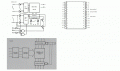
It's a 2048-word x 8 bit chip. To access all these words, I need 11 address pins, right? 2^11 gives 2048, which corresponds with the A0 to A10 pins. And each word is 8 bits long, aey?
Does this mean this chip is a "perfect" fit for an 11 bit computer? Mine is 8 bits, so I can access 256 words of these 2048, If my logic is correct.
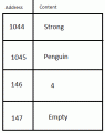
When I write in C (I try...) "int StrongPengin = 4;", does this number 4 then occupy an entire row (can I say word?) and an address with it? The variable name StrongPenguin, does this also get it's word spaces? I am assuming this would take up quite a few rows. Does the computer store it is chronological order, like I did in my drawing, or is it just random? Please see the second attachment.
I made some Paint drawings, trying to brush up the sloppy datasheets I found.
The thing is, I can't find a decent datasheet on how this works, and I can't find articles where other people have fiddled (upon writhing this, I did, but I'd rather give this a go myself at first) with this chip. I have never worked with memory before, so I know very little about this, other than what I've read today.
How do I use the row- and column decoder?
It's a 2048-word x 8 bit chip. To access all these words, I need 11 address pins, right? 2^11 gives 2048, which corresponds with the A0 to A10 pins. And each word is 8 bits long, aey?
Does this mean this chip is a "perfect" fit for an 11 bit computer? Mine is 8 bits, so I can access 256 words of these 2048, If my logic is correct.
When I write in C (I try...) "int StrongPengin = 4;", does this number 4 then occupy an entire row (can I say word?) and an address with it? The variable name StrongPenguin, does this also get it's word spaces? I am assuming this would take up quite a few rows. Does the computer store it is chronological order, like I did in my drawing, or is it just random? Please see the second attachment.
I made some Paint drawings, trying to brush up the sloppy datasheets I found.
Attachments
-
 124.8 KB Views: 9
 -
 4.7 KB Views: 8


")


