Facebook
 Google
 GitHub
 Linkedin
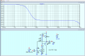
So , why is that gain is different from the feedback ? Or do I calculate it wrong ?Hi d,
This is the result for stepping R5. [Blue plot is R5=10R]
Try it for, say R2.
E
View attachment 329824
Push pull amplifier biasing
- Thread starter demir-ali
- Start date