As it shows here , Rout must be around 450ohm , so the gain must be around 20. But the swing at Va is around 2*150mv (15 gain) , and swing at vj is 2*100mv. It might be due to feedback.
That's what I learned too. This is from one of my textbooks (Manera):
It says diodes, instead of resistors, are used for biasing because they have the added benefit of tracking Vbe changes with temperature.
Hi , I was practicing the pushpull amplifier , then I figured out that circuit performs better without diode biasing. I share my simulation with you. If it is not , at least I think it should be not better , can you explain me please ? View attachment 329783
The circuit may seem to work better without the diodes, and in fact it may work 'better', but the power dissipation will be much higher. That's because the diodes help to control how hard one transistor is turned 'on' while the other transistor is turned on.
As the signal goes through zero, one transistor is required to turn 'on' while the other transistor is required to turn 'off'. When that happens, the output is assumed to be right while at the same time the power dissipation in the 'off' transistor is zero.
In practice, this exact situation, although being ideal, ends up causing distortion because of the drop in each base emitter diode. It takes time for the signal to reach the required level of the input voltage for each transistor. By keeping a small bias across the base emitter diode of the 'off' transistor, it can turn on faster once that transistor is required to turn 'on'. The capacitors maintain that bias, while the diodes limit it. That means the transistors always stay on a little even when 'off'.
This keeps the distortion to a minimum while also keeping them ready to turn on harder fast.
In the attachment, I've drawn the same circuit with the diode connections slightly different. This is equivalent to the original circuit you posted with Q3 and Q4. You can see how each diode is effectively in parallel with their respective transistors base emitter diode. Each capacitor maintains a bias for each transistor even when they are not supposed to be conducting any current to the output, while each diode limits that bias level to reduce power dissipation.
Consider what happens without the diodes. That means that when the correct transistor is conducting hard to produce an output, the other transistor is also conducting hard even though it does not have to produce any output. That raises the power dissipation in the 'off' transistor and thus it can get much hotter than it has to.
The whole idea with transistors used for linear amplifiers is to get them biased correctly. The two capacitors and the two diodes are one solution to that. There are other solutions too you can look up on the web.
That's what I learned too. This is from one of my textbooks (Manera): View attachment 329903
It says diodes, instead of resistors, are used for biasing because they have the added benefit of tracking Vbe changes with temperature.
The diodes themselves do not reduce crossover distortion.
In the process of attempting to reduce crossover distortion, it is necessary to keep the two transistors turned on at least a little bit, never allowing them to turn completely off at any time. Thus, the associated biasing resistors actually provide that function while the diodes just limit the bias levels so that one transistor does not turn on too hard while the other one is producing the actual output other half cycle.
So the diodes are involved in the limiting action of the biasing mechanism. You can reduce crossover distortion without the diodes, but the power dissipation in the transistors will go up and thus they will overheat more easily.
The better description for the diodes is that they lower power dissipation by limiting the bias current.
Notice that the description in the text:
"The diodes provide forward bias to TR2 and TR3 so as to reduce crossover distortion"
is technically incorrect. The diodes do not produce power only the power supply does, and so any forward bias must come from the power supply and that is through the resistor at the top connected to the base of the upper transistor (looks like R8).
So R8 produces the bias, the diodes just limit that bias so as to reduce power dissipation.
We could say that the diodes play a part in reducing the crossover distortion, but they do not provide any forward bias current they actually limit that current.
The circuit may seem to work better without the diodes, and in fact it may work 'better', but the power dissipation will be much higher. That's because the diodes help to control how hard one transistor is turned 'on' while the other transistor is turned on.
As the signal goes through zero, one transistor is required to turn 'on' while the other transistor is required to turn 'off'. When that happens, the output is assumed to be right while at the same time the power dissipation in the 'off' transistor is zero.
In practice, this exact situation, although being ideal, ends up causing distortion because of the drop in each base emitter diode. It takes time for the signal to reach the required level of the input voltage for each transistor. By keeping a small bias across the base emitter diode of the 'off' transistor, it can turn on faster once that transistor is required to turn 'on'. The capacitors maintain that bias, while the diodes limit it. That means the transistors always stay on a little even when 'off'.
This keeps the distortion to a minimum while also keeping them ready to turn on harder fast.
In the attachment, I've drawn the same circuit with the diode connections slightly different. This is equivalent to the original circuit you posted with Q3 and Q4. You can see how each diode is effectively in parallel with their respective transistors base emitter diode. Each capacitor maintains a bias for each transistor even when they are not supposed to be conducting any current to the output, while each diode limits that bias level to reduce power dissipation.
Consider what happens without the diodes. That means that when the correct transistor is conducting hard to produce an output, the other transistor is also conducting hard even though it does not have to produce any output. That raises the power dissipation in the 'off' transistor and thus it can get much hotter than it has to.
The whole idea with transistors used for linear amplifiers is to get them biased correctly. The two capacitors and the two diodes are one solution to that. There are other solutions too you can look up on the web.
Let us go over some basic transistor amplifier configurations so that you have a better understanding of amplifier design.
Q1 is configured as a common emitter amplifier. It provides both voltage gain and current gain. It also produces phase inversion, i.e. it inverts the signal.
Q2 is a common collector or emitter follower. It provides current gain. The voltage gain is less than unity. The output signal is not inverted.
Base bias resistors
In order for the transistor to be operating in the linear region, the base-emitter voltage must be set to about 0.65 V.
R1 supplies a base current from the supply rail. This simple bias arrangement is not recommended because the base current is very dependent on the temperature of the base-emitter junction. As the temperature increases, the base-emitter voltage drops. This further increases the collector current and the temperature rises. This is positive feedback leading to thermal run-away.
With Q2, resistors R3 and R4 create a voltage divider from the supply rail. This creates a "stiff" base-emitter voltage.
Negative Feedback
Note the minor alterations in these two circuits compared to the previous two circuits.
Base bias resistor R1 gets its source from the collector node of Q1. Since the output signal is out of phase with the input single, this constitutes negative feedback. The first consequence is that the voltage gain of this circuit is lower than that of its predecessor.
Negative feedback is beneficial because:
1) It helps to prevent thermal run-away.
2) It improves linearity.
3) It makes the circuit performance less dependent on transistor characteristic.
Q2 also has negative feedback with the inclusion of resistor R6 at the emitter.
As the current through R6 increases, so does the voltage at the emitter. This reduces the base-emitter voltage, i.e. negative feedback.
Push-Pull Output Stage
Now that we have a brief introduction of how to bias a transistor with negative feedback, let us look at the push-pull output stage of an amplifier.
R4 and R5 are retained at the emitters to provide some negative feedback. In an audio power amplifier design, the value of R4 and R5 are very low, usually between 0.1 Ω and 10 Ω.
Both transistors Q1 and Q2 are emitter followers. They work in a see-saw fashion. When one transistor is turned on, the other transistor is turned off. This is where cross-over distortion rears its ugly head. In order in reduce cross-over distortion, we need to shift the transistor amplifier from Class-B towards Class-A, i.e, Class-AB.
To accomplish this, we need to increase the value of R2, i.e. increase the voltage difference between the two base voltages. The down side is that power consumption is increased. We have to a make a compromise between idle power consumption and cross-over distortion.
A good idea is to replace R2 with two diodes in series. This provides a voltage difference of two forward bias diodes, i.e. about 1.3 V.
You can take this one extra step by retaining resistance R2 in series with the two diodes. You can ignore R2 if the amount of cross-over distortion is not noticeable.
Now we can add the driver stage in order to provide some voltage gain to the circuit.
Note again, R6 provides negative feedback which is very beneficial as outlined before.
There you have it, a simple description on how to design a simple driver and push-pull output stage for an audio amplifier design.
With audio amplifiers, including complementary ones, there is always a compromise between efficiency and distortion. Crossover distortion is a challenge indeed. I suggest studying the output sections of good quality audio amplifiers to see how a solution is reached, and then using a simulator to evaluate the effects of changes to the component values. It is often possible to learn a lot from observing how others have succeeded.
I'd say that the compromise was between efficiency, distortion and complexity.
It is possible to make a pure Class B perform well, if the output transistors are fast (Ft>30MHz) and the gain of the input stage is large enough and the compensation is arranged to that it doesn't slug the voltage amplifier stage. SPICE says this circuit has distortion <-110dB (0.0003%) for the second harmonics. All other harmonics are <-120dB, so are unlikely ever to be audible.
Q1 is configured as a common emitter amplifier. It provides both voltage gain and current gain. It also produces phase inversion, i.e. it inverts the signal.
Q2 is a common collector or emitter follower. It provides current gain. The voltage gain is less than unity. The output signal is not inverted.
In order for the transistor to be operating in the linear region, the base-emitter voltage must be set to about 0.65 V.
R1 supplies a base current from the supply rail. This simple bias arrangement is not recommended because the base current is very dependent on the temperature of the base-emitter junction. As the temperature increases, the base-emitter voltage drops. This further increases the collector current and the temperature rises. This is positive feedback leading to thermal run-away.
With Q2, resistors R3 and R4 create a voltage divider from the supply rail. This creates a "stiff" base-emitter voltage.
Negative Feedback
View attachment 329914
Note the minor alterations in these two circuits compared to the previous two circuits.
Base bias resistor R1 gets its source from the collector node of Q1. Since the output signal is out of phase with the input single, this constitutes negative feedback. The first consequence is that the voltage gain of this circuit is lower than that of its predecessor.
Negative feedback is beneficial because:
1) It helps to prevent thermal run-away.
2) It improves linearity.
3) It makes the circuit performance less dependent on transistor characteristic.
Q2 also has negative feedback with the inclusion of resistor R6 at the emitter.
As the current through R6 increases, so does the voltage at the emitter. This reduces the base-emitter voltage, i.e. negative feedback.
Push-Pull Output Stage
Now that we have a brief introduction of how to bias a transistor with negative feedback, let us look at the push-pull output stage of an amplifier.
R4 and R5 are retained at the emitters to provide some negative feedback. In an audio power amplifier design, the value of R4 and R5 are very low, usually between 0.1 Ω and 10 Ω.
Both transistors Q1 and Q2 are emitter followers. They work in a see-saw fashion. When one transistor is turned on, the other transistor is turned off. This is where cross-over distortion rears its ugly head. In order in reduce cross-over distortion, we need to shift the transistor amplifier from Class-B towards Class-A, i.e, Class-AB.
To accomplish this, we need to increase the value of R2, i.e. increase the voltage difference between the two base voltages. The down side is that power consumption is increased. We have to a make a compromise between idle power consumption and cross-over distortion.
A good idea is to replace R2 with two diodes in series. This provides a voltage difference of two forward bias diodes, i.e. about 1.3 V.
You can take this one extra step further by retaining resistance R2 in series with the two diodes.
Now we can add the driver stage in order to provide some voltage gain to the circuit.
Note again, R6 provides negative feedback which is very beneficial as outlined before. View attachment 329924
There you have it, a simple description on how to design a simple driver and push-pull output stage for an audio amplifier design.
I'd say that the compromise was between efficiency, distortion and complexity.
It is possible to make a pure Class B perform well, if the output transistors are fast (Ft>30MHz) and the gain of the input stage is large enough and the compensation is arranged to that it doesn't slug the voltage amplifier stage. View attachment 329925View attachment 329926SPICE says this circuit has distortion <-110dB (0.0003%) for the second harmonics. All other harmonics are <-120dB, so are unlikely ever to be audible.
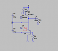
Hi, I comment on parts of circuit , and pointed the part that I could not get how it works. I did not make any detailed analyses another than commenting as I am strange with these topologies. Can you correct me or explain please ?
R15 is the input bias resistor (it does nothing in the SPICE simulation)
2 is the feedback from output to the inverting input
3 is a bootstrap current source.
Have a look at these scans from Linsley-Hood's book.
R15 is the input bias resistor (it does nothing in the SPICE simulation)
2 is the feedback from output to the inverting input
3 is a bootstrap current source.
Have a look at these scans from Linsley-Hood's book.
The capacitor keeps the voltage across R3 almost constant. Constant voltage across constant resistance = constant current.
The feedback gives unity gain at DC and a gain of 11 at AC.
Sorry, I can't find the Linsley-Hood scans. I'll scan them again tomorrow - they are worth the wait!
 Facebook
 Google
 GitHub
 Linkedin


")


