I will check them , I will wait for sure because I am having fun spending my time over these. Actually feedbacks and amplifiers are generally my next semesters subject but I am having fun with working these , making experiments.
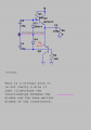
That circuit was not meant to be taken literally it was just to show the relationships between the diode voltages and the transistor base emitter voltages. I'll redraw it to make it more clear though thanks for the heads up.
Those added connections are not really meant to be wired into the circuit, they just show the voltage relationships between the diodes and the transistor base emitter junctions. The theory is that the diodes have the same voltage drop as the base emitter diodes. It's an approximation so you might better see why they are there.
However, here is a better diagram ... but be aware those violet wires are virtual they are not meant to be wired into the circuit.
The diodes themselves do not reduce crossover distortion.
In the process of attempting to reduce crossover distortion, it is necessary to keep the two transistors turned on at least a little bit, never allowing them to turn completely off at any time. Thus, the associated biasing resistors actually provide that function while the diodes just limit the bias levels so that one transistor does not turn on too hard while the other one is producing the actual output other half cycle.
So the diodes are involved in the limiting action of the biasing mechanism. You can reduce crossover distortion without the diodes, but the power dissipation in the transistors will go up and thus they will overheat more easily.
The better description for the diodes is that they lower power dissipation by limiting the bias current.
Notice that the description in the text:
"The diodes provide forward bias to TR2 and TR3 so as to reduce crossover distortion"
is technically incorrect. The diodes do not produce power only the power supply does, and so any forward bias must come from the power supply and that is through the resistor at the top connected to the base of the upper transistor (looks like R8).
So R8 produces the bias, the diodes just limit that bias so as to reduce power dissipation.
We could say that the diodes play a part in reducing the crossover distortion, but they do not provide any forward bias current they actually limit that current.
Goodness me, Mr Al, you are making this biasing thing a mountain out of a molehill.
Resistors can bias the transistors - but they need current to do so, and no-one uses resistors any more to bias a Class AB amplifier because they do not provide any thermal compensation. Diodes are a mixed blessing, but to provide the current needed to avoid crossover distortion (instead of a resistor) they need to provide a match similar to the Vbe of the transistor(s) they are supposed to be biasing. And as mentioned, diodes are used because they can both provide the bias needed AND provide some degree of thermal matching as the Vbe and Vf change with temperature.
What is used, as I am sure you know, is some form of transistor bias generator. That is usually trimmable and provides an adjustment to set the bias current and provide compensation at the same time.
Your continued insistence that "resistors can minimise crossover distortion" is not untrue but it is not the way things are done. Because they won't provide a stable situation with temperature.
I am not sure you understand what I was saying. Resistors alone do not make up the bias circuit but the current flow through them is the actual bias current, not the current through the diodes. We use resistors to provide this current flow because a diode voltage drop is too abrupt. We do however use diodes to limit this current flow because they do a reasonable job of shunting some of that current away from the BE junction when needed.
The resistors allow the power supply to supply the current, the diodes cannot supply current and they do not conduct in order to supply bias current they conduct to LIMIT bias current.
I do agree that the diodes forward voltage, in theory and if perfect, would have to be a match for the transistor Vbe. They are not a perfect match ever so sometimes other means are also employed as I am sure you know. I am not a big fan of the bias scheme presented, but it was presented so it was talked about.
When we talk about these circuits we talk about these circuits and that means bringing out as many facts as possible so anyone reading can see the whole picture, and we try to make that picture as perfect as possible. That often means increasing the level of detail.
OK, the fact is that the diodes ARE PART OF THE CIRCUIT USED TO REDUCE CROSSOVER DISTORTION!
I am amazed that such an argument could go on so far. Sheesh!!!
OK, the fact is that the diodes ARE PART OF THE CIRCUIT USED TO REDUCE CROSSOVER DISTORTION!
I am amazed that such an argument could go on so far. Sheesh!!!
Yo, can you help me calculate the gain in this circuit ?
I do use gm*Rc but it does not work. Lowering the base bias resistors made some difference. DRAFT8.asc file is for this.
Edit : I also made an cascode amplifier. Can this be used as preamplifier ? Draft9.asc is this
In theory, the gain will be around Av = 0.5*gm*Rc. But we have to consider R4 influence.
If we assume that the transistor beta is 500 we have this gain expression: Av ≈ 0.5 * Rc/( 1/gm + R4/500) = 0.5 * 10k/(50.8Ω + 66Ω) ≈ 43V/V
Also, next time try to use Ctrl+E in LTspice to mirror the component and Ctrl+R to rotate one.
Since Vin is not out input and it is a diff pair , I might be approaching it in a wrong way but , since emitter is Ac Gnd , why do we use that formula ?
Since Vin is not out input and it is a diff pair , I might be approaching it in a wrong way but , since emitter is Ac Gnd , why do we use that formula ?
Notice that the Q1 base is the input and Q2 collector we have an output. Therefore, Q1 is an emitter follower (common collector) and Q2 is a common base amplifier stage.
Your small-signal model is wrong. And the emitters are not at AC GND.
Notice that the Q1 base is the input and Q2 collector we have an output. Therefore, Q1 is an emitter follower (common collector) and Q2 is a common base amplifier stage.
Your small-signal model is wrong. And the emitters are not at AC GND.
A differential amp works by the AC voltage being common on the two emitters, so the voltage on one transistor affects the current on the other transistor in the opposite direction (hence differential).
If you AC ground the emitters, then there is no AC signal on the two emitters and thus they no longer act as an AC differential stage, instead just two separate AC amplifiers (but they still work as differential at DC).
This is just a first-order approximation that works only if you have a fully symmetrical circuit. And fully symmetrical input voltage applies to both bases.
This is just a first-order approximation that works only if you have a fully symmetrical circuit. And fully symmetrical input voltage applies to both bases.
True, the linear region is small due to the exponential behavior of Vbe vs Ic. And ss the name suggests the differential amplifier "reacts" to a voltage difference between two bases.
\[ \frac{I_{E1}}{I_{E2}} = e^{\frac{V_{BE1}- V_{BE2}}{26mV}} \]
But I'm sure books mention about it too.
 Facebook
 Google
 GitHub
 Linkedin