Practical Circuit Construction

Thread Starter

Kittu20

Joined Oct 12, 2022
470
I am a newbie, Before that I have not practically implemented any circuit on Vero board,

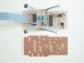
I am interested in making electronic circuits practically. I've collected some stuff for this. I want to make development board on Vero board. The board has two parts, one is the top and the other is the bottom. I would like to place all the components on the top side and I would like to route the components on the bottom.

I want some tips and advice from you guys on how to connect the components on the bottom side. Should I use wire to connect the components or make rails of soldering flux to connect each other?
 

Attachments

Audioguru again

Joined Oct 21, 2019
6,692
I made many circuit modules on Veroboard (stripboard).
The parts and a few short jumper wires are all on the parts side. No wires on the bottom side of the board because the strips form most of the wiring.
The strips are cut to short lengths with a Veroboard strip cutter tool or a drill bit. Then many or a few sections of each strip are used for different wiring in the circuit.
 

Attachments

MrChips

Joined Oct 2, 2009
30,810
Welcome to AAC!

There are different layouts used for prototyping boards. Bertus has shown examples in post #2.
Veroboard is a registered brand name, and so is Vector. The first photo shown by Bertus is the original Veroboard.
Don't call it Veroboard unless it is a board made by Vero. Call it prototyping board instead.

What you have shown in your original post is single point solder pads, something like this:

1665685196545.png

There are different layouts for different applications.
If you are employing a lot of DIP (dual in-line package) ICs, then something like this is easier to use:
1665685314156.png

If you want to use what you have there are a number of options.

1) You can run bare copper wires in the bottom side.
1665685597867.jpeg

2) You can run plastic insulated #24 AWG or #30 AWG wire-wrap wire on the topside or bottom side:
1665685596505.png

Personally, I like neither of the above. I prefer to run wire-wrap wire on the topside using the layout suited for DIP ICs.
Something like this:
1665686096163.png

For simple small projects I prefer to use the original Veroboard. With strategic planning you can minimize the number of jumpers required from component led to component lead.

If you have a large number of DIP ICs on the board, wire-wrap sockets is much more convenient and faster to use.
The 3M IDC system is best for large CPU style bus systems. Unfortunately they are no longer available.
 

MrSalts

Joined Apr 2, 2020
2,767
I prefer drawing out the board, paying $40 to $50 to get my completed, professionally made circuit board fabricated and shipped to me via DHL or FedEx from China in, typically, 8 to 10 days from order payment. Way better and simpler than spending tedious hours cutting wires, soldering, trying to keep track of what goes where with all the jumper wires. The best part of my plan, is that you typically get 5 to 10 PCBs for that price. Much more productivity because, it takes about 1/10th the time to just solder the components and not worry about connecting all the nodes with jumpers, drilling or cutting strips. But, my time is valuable to me and I am willing to spend money to save time, not sit at a workbench by myself doing what I view as tedious work. Other people have different views - they may value their money more than I do and their time less than I do. They may even enjoy filling their free time with this type of work - and all of that is ok - your decision.
 

MaxHeadRoom

Joined Jul 18, 2013
28,688
I am a newbie, Before that I have not practically implemented any circuit on Vero board,
Should I use wire to connect the components or make rails of soldering flux to connect each other?
If you use true Vero board as in Bertus first item in the post, it makes the job a lot easier than the example you show in your pic.
That is my choice anyway, for one-off's .
 

MrChips

Joined Oct 2, 2009
30,810
You can make it as unreliable or reliable as you wish. Personally it looks messy and a pain to do.
I prefer to use the real Veroboard. Here is an example.

1665709875090.png
 

dl324

Joined Mar 30, 2015
16,922
I want some tips and advice from you guys on how to connect the components on the bottom side. Should I use wire to connect the components or make rails of soldering flux to connect each other?
Use a schematic editor that supports board layout. Layout your components as if you were going to make a board to optimize component placement and minimize wire crossings.

The board you showed is a double sided pad-per-hole board. I prefer boards with only holes, but have been using single sided pad-per-hole phenolic boards. I put the pads on the component side so I wouldn't have to worry about bare wire connections getting shorted by the pads. The power rails are the 3 copper wires in the center; some power is elevated from the other wires.
6discreteFlipFlops.jpg6discreteFlipFlopsComponentSide.jpg

I did the layout in Eagle:
4discreteFFBot.jpg4discreteFFComp.jpg
The board layout was for 4 flip flops that I modified on the fly to be 6 flip flops to avoid wasting any board area.

If I was going to do more than one board, I'd make some boards using the toner transfer method. Different board:
tonerTransfer1.jpg

You might want to invest in a better soldering iron.

Use a tool like this to form leads on axial components:
jamecoLeadFormer.jpg
Use needle nose pliers to bend the leads on the LEDs. You want to avoid stressing them at the package.
 
Last edited:

ScottWang

Joined Aug 23, 2012
7,400
Welcome to AAC!

There are different layouts used for prototyping boards. Bertus has shown examples in post #2.
Veroboard is a registered brand name, and so is Vector. The first photo shown by Bertus is the original Veroboard.
Don't call it Veroboard unless it is a board made by Vero. Call it prototyping board instead.

What you have shown in your original post is single point solder pads, something like this:

View attachment 278311

There are different layouts for different applications.
If you are employing a lot of DIP (dual in-line package) ICs, then something like this is easier to use:
View attachment 278312

If you want to use what you have there are a number of options.

1) You can run bare copper wires in the bottom side.
View attachment 278314

2) You can run plastic insulated #24 AWG or #30 AWG wire-wrap wire on the topside or bottom side:
View attachment 278313

Personally, I like neither of the above. I prefer to run wire-wrap wire on the topside using the layout suited for DIP ICs.
Something like this:
View attachment 278319

For simple small projects I prefer to use the original Veroboard. With strategic planning you can minimize the number of jumpers required from component led to component lead.

If you have a large number of DIP ICs on the board, wire-wrap sockets is much more convenient and faster to use.
The 3M IDC system is best for large CPU style bus systems. Unfortunately they are no longer available.
Haha ... :)
They look like some kind of Demo board for teaching
 
I made many circuit modules on Veroboard (stripboard).
The parts and a few short jumper wires are all on the parts side. No wires on the bottom side of the board because the strips form most of the wiring.
I very much favour this approach. I wish I was as neat as Audioguru! I've attached a pdf of a paper template made in Excel which I use for doing layouts. I use https://uk.rs-online.com/web/p/copper-wire/0355079 for .connecting links.

1665749183620.jpeg

1665749204728.jpeg
I urge you not to get in the habit of using those ghastly solderless prototyping boards for anything other than testing whether an idea with just a few components actually works before building the whole circuit on stripboard.
 

Attachments

atferrari

Joined Jan 6, 2004
4,770
While my provison of Veroboard lasted I used them for projects that I considered more or less in final stage. Later, buying them abroad became an expensive, risky option, typical of a ridiculous country.

This is from a youtuber EE that I suscribed to long ago:


dl324

Joined Mar 30, 2015
16,922
I urge you not to get in the habit of using those ghastly solderless prototyping boards for anything other than testing whether an idea with just a few components actually works before building the whole circuit on stripboard.
Why is that?

I breadboarded this years ago and still haven't gotten around to making a board for it.
1665760151276.png
 

dl324

Joined Mar 30, 2015
16,922
Simple.
When the cat (or mouse or whatever) pulls out a single wire it takes a hell of a long time trying to out why it does not work.
#22 wire doesn't pull out that easily; though I used some #24 in this circuit. If that happens, I just use typical troubleshooting procedures.
 

atferrari

Joined Jan 6, 2004
4,770
All my projects and I mean ALL, including a micro since the venerable 16C57 were initially implemented on breadboards.

Have to admit that the firsts I used were ACE branded of a superb quality. IIRC they called them "protboards". Now I stick to Chinese quality level but I am more careful to not make them more unreliable.
 

ericgibbs

Joined Jan 29, 2010
18,849
hi JHT
Like dl324 I have bread board circuits working for years in out-buildings, MCU's running at 20MHz , HC12 TRX links etc, no problems.
E
 
Top