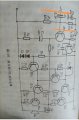
They form a "quiet" bias voltage for the input transistor. C2/R3 is a low-pass filter at an unspecified frequency as there is no value for R2 on the diagram, but it would be <<50Hz. This removes power supply ripple and other noise from the bias voltage for BG1. Without it, the amplifier would amplify the power supply ripple and it would find its way to the output.
Point A will be stable. Point B will have the input signal, JUST the input signal and no contribution from power supply ripple and noise, because it is biassed from point A which is stable.
For the input to get to point B it passes through a high-pass filter formed of C1 and R1||R2 (in parallel) which cuts off below 2.7Hz thus removing any DC component
The amplifier main supply voltage might have hum, other noises or be jumping up and down from output current affecting the voltage.
The resistor and capacitor filter the voltage fed to the first transistor so that the entire circuit does not amplify the noises or break into oscillation from it.
I made your schematic smaller and turned it so that it is not sideways.
It is unfortunate that when we get some schematics they often can not show every single little thing that affects the circuit operation. There are always assumptions that are not explicitly illustrated. IT takes some experience before we can understand some of the more subtle points of how the circuit operates and thus why circuit parts are present or absent.
In this case, the amplifier power supply is NOT shown at all. This means we can not know the actual output impedance and this the effect a load has on the voltage output of that power supply. However, we would know from experience that most power supplies have an output that decreases somewhat when a load is applied, and also if that load is changing then the output voltage will be changing. When we see just the amplifier schematic, it looks like the power supply is perfect but it's not it has limitations and those limitations can not be known without seeing the drawing for that power supply.
Without that info, we assume that the power supply loads down by some amount and this causes the voltage to decrease, and as the load changes teh voltage fluctuates.
Now with that in mind, follow the connection from the power supply input to the resistor R3 and capacitor C2 as you point out. If we didnt hve that, the power supply would be connected directly to the bias resistor. That would mean the bias would be changing based on the loading effect of the power supply and that would most likely cause an extra unwanted input signal when all we want is the actual input signal.
With the resistor and capacitor, the fluctuations from the power supply are not felt as much at the input because the capacitor C2 filters that out. It's not perfect (often an inductor is included also) but it's a lot better than nothing. So you get a better, cleaner, output.
There is a noteworthy variation on this theme. The power supply sometimes has output hum from the line frequency and sometimes some hum from the line frequency is present at the input anyway and since the input is so sensitive to small changes the hum would get amplified. To help lower the effect of this, sometimes a conditioned part of the line frequency is purposely injected into an input, and because it will be inverted from the unwanted hum it will help to reduce the total hum that gets amplified. This was often done on tube type amplifiers so you could actually tune out the hum which made it much lower.
If you still want to know about the bias setting: https://forum.allaboutcircuits.com/threads/semicomplementry-otl-power-amplifier.186877/#post-1732915
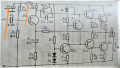
You need about about 12.5mV across R14 to give 25mA bias. The bias can increase to 100mA with no ill-effects apart from its running a bit warm.
Add to that Vbe[BG5] and Vbe[BG7] and that gives the voltage at BG3 collector, compared to the output (collector of BG8)
BG3 emitter will be Vbe[BG6] negative of the output, plus a tiny voltage across R12.
The absolute voltages are not important, it is the difference between them that matters.
BG3 is a Vbe-multiplier. It is explained very well here: https://sound-au.com/amp_design.htm#s32
Because the adjustment is very sensitive to the actual values of Vbe, R9 is usually a preset.
The rest of the article is worth reading as well.
 Facebook
 Google
 GitHub
 Linkedin

 459 KB Views: 2

")


