Facebook
 Google
 GitHub
 Linkedin
So just exchange the source and load, with the load being the fixed resistor.You are using the Maximum Power Transfer Theorem to make say things that it says nothing about. The theorem ONLY talks about maximizing power transfer to a load. It says absolutely nothing, zero, nada, about power dissipation in the source.
So when the output power is maximum, its the same as the source power dissipation under the circumstances of this discussion, which is implied by the Maximum Power Theorem.
But if you want to be pedantic about it, I can't stop you.
It is not, and I don't understand why you think it is.Your entire premise is that the power dissipated in this equivalent resistance is the same as the actual power dissipated in the actual opamp internal circuitry. That equivalence is the fallacy.
Explain the fallacy, since you haven't so far, other than just waving your arms about the Maximum Power Transfer Theorem and Thevenin equivalents, as if I don't understand those concepts.
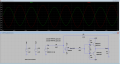
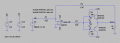
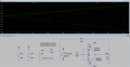
Can we agree that the op amp power dissipated (ignoring its bias power) is simply the difference between the supply voltage and the output voltage times the output current?
The maximum for this occurs when the op amp equivalent resistance equals the load resistance and the output voltage equals 1/2 the supply voltage (as shown in my sim).
How is that a fallacy?
Last edited: