That is a SERIES connection, not a pull up. Series is what you want. But I don't see ANY wires.
Why not use a resistor between the port pin and one of the LEDs on your development board??
You have buttons on that board too.
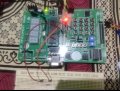
Schematic shows only one resistor pack RP1 - I suspect that the schematic lies
Board has two 5-pin resistor packs, but hard to be certain what the second one does
Keep using your breadboard resistor until you can post a picture of the board underside
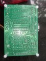
Schematic shows only one resistor pack RP1 - I suspect that the schematic lies
Board has two 5-pin resistor packs, but hard to be certain what the second one does
Keep using your breadboard resistor until you can post a picture of the board underside
 Facebook
 Google
 GitHub
 Linkedin