Facebook
 Google
 GitHub
 Linkedin
Hello,
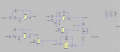
I am new to hardware design. I am designing measurement circuit for Impedance Spectroscopy of electrochemistry cell. I need to measure the current coming from electrodes which have range from few milliamperes to few nanoamperes. as literature suggested, the equivalent circuit for electrochemistry cell can be seen below.

schematic of Transimpedance Amplifier given below with additional circuit of Potensiostat to control the voltage at ref_v1 in the schematic.

I have calculated Rf and CF of TIA from formulas given in the datasheet of ADA4530. please note that R2 and C2 in the circuit which is equivalent circuit of electrochemistry varies and unknown to me. Therefore I am varying R2 from 100 ohms to 1Mohms with steps of multiple of 10 and C2 from 1pf to 1uf with step of multiple of 10 just for the simulation. That is why, I have to vary RF and CF of TIA so that it would be stable and cover huge current range.
Now, I have problem with phase and gain. for e.g. scenario 1: if my R2 = 1Mohms and C2=1nf and Rf=1Mohms and Cf= 23pf then phase of the transfer function is -90.65 degree at 100kHz and I believe that it must be close to -180 degree. because if I want to calculate impedance of equivalent circuit then with -90.65 degree I would have error in impedance calculation. at lower frequency I got very low gain hence voltage measurement could not possible. please also note that gain at higher frequencies is so high that noise could go up to approx. 80uV/sqrt(Hz)(I didn't attach the picture ). it can be seen below.


scenario 2: when I change Rf to 10k then I get 'good' phase response and in high frequencies, output voltage is acceptable but in low frequencies, output voltage is very low. it can be seen below

from above two scenarios, I believe that with different value of CF and Rf, zeros and poles is being added in 100k bandwidth which change the group delay.
My question is, how I could get flat gain response(not absolutely necessary) and flat group delay(absolutely necessary) of 100kHz bandwidth (like bessel response)?
input volatge ('input' tag in schematic) = 100mv AC signal. Frequency range: 1Hz - 100Khz. GBP of ADA4530: 2Mhz
Note: I have written C code to calculate RF and CF values for different C2 and R2 and selected values according to ADA4530 datasheet. please let me know, if you need other specifications or information.
Thank you.
Attachments
-
 2.3 KB Views: 4
 -
 38.9 KB Views: 4