pcb design layout

Thread Starter

bry1007

Joined May 27, 2025
1
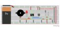
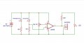
Can I get some help with creating a PCB layout for our electronics project? Our professor provided us with a schematic diagram, but we weren't taught how to design the layout on a PCB. I've included the diagram below. Could someone help with the layout design?

the materials used are:
lm358 ic
ir transmitter receiver
buzzer
led
10k ohms variable resistor
100 ohms resistor
220 ohms resistor
10K ohms resistor
 

Attachments

MrChips

Joined Oct 2, 2009
34,806
Before laying out a PCB on a CAD program, it helps the learning process to do a layout with pencil and paper.
I like to use checkered paper and three erasable pencils or crayons, red, blue or green, and ordinary lead pencil.

1748361993981.png

Use the circuit schmatics as a starting point. Place the actual component on a piece of paper or cardboard to give you an idea of where you want the components to be placed.

Then draw the outline of the components on the checkered paper using a pencil or ink pen.
Now start placing the electrical connections with the blue crayon. Blue lines must not cross another blue line. This will be the bottom side (solder side). Try to get most of the connections resolved on this side.

Complete the connections with the red crayon. This will be the top layer or component side.

For a simple PCB layout, you can attempt to make all the connections on the blue layer alone. Any remaining connections can be done on the top layer using wire jumpers. In this case, you will produce a single sided PCB.
 

dl324

Joined Mar 30, 2015
18,326
Welcome to AAC!
we weren't taught how to design the layout on a PCB.
One way is to use the layout on the solderless breadboard as a guide using this board.
1748364644793.png
Unfortunately, you didn't place the components compactly.

When you're designing a board/solderless breadboard, the objective is to do a compact layout (preferably with components on a grid and aligned as much as possible).

EDIT: As I recall, Tinkercad fritzing has a board layout capability.

Here's a discrete MOSFET voltage regulator I designed and the corresponding layout on a solderless breadboard. The placement of the components just "fell out" from the placement of the components in the (well-drawn IMO) schematic.

discreteMosfetRegulatorFinal.jpg
discreteMosfetRegulatorFinalAsBuilt.jpg
 
Last edited:

dl324

Joined Mar 30, 2015
18,326
You have a wiring problem with the opamp inputs. The pot should go to pin 2 and the connection to the receiver LED cathode is connected to ground.
 

dl324

Joined Mar 30, 2015
18,326
We can't offer any suggestions unless you show some effort.

Correct the wiring errors and show your attempt.

BTW, how is the circuit supposed to work? It seems to me that the receive LED should be a detector and be reverse biased, the transmit LED seems extraneous, and you're using an opamp as a comparator.
 

KeithWalker

Joined Jul 10, 2017
3,606
We can't offer any suggestions unless you show some effort.

Correct the wiring errors and show your attempt.

BTW, how is the circuit supposed to work? It seems to me that the receive LED should be a detector and be reverse biased, the transmit LED seems extraneous, and you're using an opamp as a comparator.
The buzzer will sound the if an opaque object is placed between the transmitter and receiver. I agree that the receiver diode is shown connected the wrong way round in the schematic but a LM358 works well as a comparator.
 
Top