Opamp gain calculation

Thread Starter

andrew74

Joined Jul 25, 2022
245
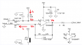
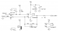
Hi everyone, this is the amplifier stage of the X-NUCLEONUCLEO-IHM08M1.
1780652442283.png


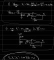
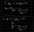
I’ve done some calculations to work out the profit, but I’m not sure what resistance value to put in the blue question marks:
SmartSelect_20260605_113554_Samsung Notes.jpg

Point 1) corresponds to the effect of Vshunt1, while point 2) corresponds to 3.3V .. in the end, I should add them up

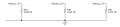
I’d also like to ask what you think is the point of placing those 3.3V pull-up resistors on the non-inverting input… perhaps because the resistor (between + and -) is connected to the source of the MOSFETs for phase current measurement.
1780652612413.png
 

ericgibbs

Joined Jan 29, 2010
21,506
I’ve done some calculations to work out the profit, but I’m not sure what resistance value to put in the blue question marks:
Hi Andrew,
For an Inverting OPA, which two resistors set the basic Gain value for the OPA.?
Post the equation you need to use.
E
 

WBahn

Joined Mar 31, 2012
33,020
Hi everyone, this is the amplifier stage of the X-NUCLEONUCLEO-IHM08M1.

View attachment 368041


I’ve done some calculations to work out the profit, but I’m not sure what resistance value to put in the blue question marks:
View attachment 368042

Point 1) corresponds to the effect of Vshunt1, while point 2) corresponds to 3.3V .. in the end, I should add them up

I’d also like to ask what you think is the point of placing those 3.3V pull-up resistors on the non-inverting input… perhaps because the resistor (between + and -) is connected to the source of the MOSFETs for phase current measurement.
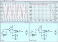
View attachment 368043
Why are you completely ignoring the effect of R4?

Instead of trying to throw memorized or looked up equations at it, just analyze the circuit.

1780674635837.png

Assuming an ideal opamp Vp = Vn.

At sufficiently low frequencies, C3 and C4 have sufficiently high impedance to be ignored. So, within that frequency realm:

Looking at the non-inverting input:

ip = (Vcc - Vs) / (R1+R2)

where Vcc = 3.3 V and Vs = Vshunt_1

Vp = Vs + ip*R2

Vp = Vs + ( (Vcc - Vs) / (R1+R2) )·R2

Vp = Vs (1 - (R2/(R1+R2))) + Vcc·(R2/(R1+R2))

Vp = Vs (R1/(R1+R2)) + Vcc·(R2/(R1+R2))

Turning to the inverting input, we have:

Vn = Vo · (R4/(R4+R5)

Now just set them equal and solve for Vo:

Vp = Vn

Vs (R1/(R1+R2)) + Vcc·(R2/(R1+R2)) = Vo · (R4/(R4+R5)

Vo = [ Vs (R1/(R1+R2)) + Vcc·(R2/(R1+R2)) ] / [(R4/(R4+R5)]

Vo = [ Vs (R1/(R1+R2)) + Vcc·(R2/(R1+R2)) ] · [1 + (R5/R4)]

We can massage this to put it in terms of ratios pretty easily:

Vo = Vs · [ (1 + (R5/R4)) ] / [ (1 + (R2/R1)) ] + Vcc · [ (1 + (R5/R4)) ] / [ (1 + (R1/R2)) ]

As a sanity check (since I'm doing all of the manipulation as I type, which history has shown is somewhat prone to making mistakes), let's see if this limits correctly.

If R1 and R4 are removed (made infinite), we have the classic non-inverting amplifier which should have a gain of (1 + (R5/R4)):

Vo = Vs · [ (1 + (R5/R4)) ] / [ (1 + (R2/∞)) ] + Vcc · [ (1 + (R5/R4)) ] / [ (1 + (∞/R2)) ]

Vo = Vs · [ (1 + (R5/R4)) ] / [ (1 + 0) ] + Vcc · [ (1 + (R5/R4) )) ] / [ (1 + ∞) ]

Vo = Vs · [ (1 + (R5/R4)) / 1 ] + Vcc · [ (1 + (R5/R4)) / ∞ ]

Vo = Vs · [ (1 + (R5/R4)) ] + Vcc · [ 0 ]

Vo = Vs · (1 + (R5/R4))

So it passes this check, which is probably good enough.

As you can see, you can't just ignore R4, as the ratio R5/R4 is what sets the gain.

In this case, the output becomes

Vo = Vs · [ (1 + (4.7 kΩ / 1 kΩ)) ] / [ (1 + (680 Ω / 6.8 kΩ)) ] + 3.3 V · [ 1 + (4.7 kΩ / 1 kΩ)) ] / [ (1 + (6.8 kΩ / 680 Ω)) ]

Vo = Vs · [ (1 + 4.7) ] / [ (1 + 0.1) ] + 3.3 V · [ (1 + 4.7) ] / [ (1 + 10) ]

Vo = Vs · ( 5.7 / 1.1 ) + 3.3 V · (5.7 / 11)

Vo = 5.18·Vs + 1.71 V

The next question is what constitutes a low enough frequency for the DC gain to be applicable to the signal.

You have two cutoff frequencies, one associated with each of the capacitors C3 and C4. To a good approximation, the one with C3 is due to the RC time constant of C3 and the parallel combination of R1 and R2, which is roughly just R2. The one with C4 is the RC time constant of C4 and the sum of R4 and R5. If I did it right, these are therefore at about 16 kHz and 280 kHz, respectively. So if you are looking only at frequencies well below 16 kHz, the DC gain should apply pretty closely.

As for the pullup resistors, I can only guess. It would seem that they might be there to provide a DC bias to the output, perhaps because the next block in the processing can't handle voltages that are too close to the rails. That's only a guess.

Your shunt resistors are 10 mΩ rated at 1 W. That means the max current is 10 A, making the max input signal just 0.1 V, which would make the output barely 0.5 V without the pullup.

in your second diagram, why are you calling those pull "up" resistors?
 

Thread Starter

andrew74

Joined Jul 25, 2022
245
Andrew - Why do you neglect the capacitors C3 and C4 in your calculation?
C4 isn't mounted; C3 acts as a low-pass filter... perhaps I should switch to Laplace and include it in the calculations?
I think the frequency of the phase currents is low enough that we can ignore C3 .. for now
 

Futurist

Joined Apr 8, 2025
879
Why are you completely ignoring the effect of R4?

Instead of trying to throw memorized or looked up equations at it, just analyze the circuit.

View attachment 368046

Assuming an ideal opamp Vp = Vn.

At sufficiently low frequencies, C3 and C4 have sufficiently high impedance to be ignored. So, within that frequency realm:

Looking at the non-inverting input:

ip = (Vcc - Vs) / (R1+R2)

where Vcc = 3.3 V and Vs = Vshunt_1

Vp = Vs + ip*R2

Vp = Vs + ( (Vcc - Vs) / (R1+R2) )·R2

Vp = Vs (1 - (R2/(R1+R2))) + Vcc·(R2/(R1+R2))

Vp = Vs (R1/(R1+R2)) + Vcc·(R2/(R1+R2))

Turning to the inverting input, we have:

Vn = Vo · (R4/(R4+R5)

Now just set them equal and solve for Vo:

Vp = Vn

Vs (R1/(R1+R2)) + Vcc·(R2/(R1+R2)) = Vo · (R4/(R4+R5)

Vo = [ Vs (R1/(R1+R2)) + Vcc·(R2/(R1+R2)) ] / [(R4/(R4+R5)]

Vo = [ Vs (R1/(R1+R2)) + Vcc·(R2/(R1+R2)) ] · [1 + (R5/R4)]

We can massage this to put it in terms of ratios pretty easily:

Vo = Vs · [ (1 + (R5/R4)) ] / [ (1 + (R2/R1)) ] + Vcc · [ (1 + (R5/R4)) ] / [ (1 + (R1/R2)) ]

As a sanity check (since I'm doing all of the manipulation as I type, which history has shown is somewhat prone to making mistakes), let's see if this limits correctly.

If R1 and R4 are removed (made infinite), we have the classic non-inverting amplifier which should have a gain of (1 + (R5/R4)):

Vo = Vs · [ (1 + (R5/R4)) ] / [ (1 + (R2/∞)) ] + Vcc · [ (1 + (R5/R4)) ] / [ (1 + (∞/R2)) ]

Vo = Vs · [ (1 + (R5/R4)) ] / [ (1 + 0) ] + Vcc · [ (1 + (R5/R4) )) ] / [ (1 + ∞) ]

Vo = Vs · [ (1 + (R5/R4)) / 1 ] + Vcc · [ (1 + (R5/R4)) / ∞ ]

Vo = Vs · [ (1 + (R5/R4)) ] + Vcc · [ 0 ]

Vo = Vs · (1 + (R5/R4))

So it passes this check, which is probably good enough.

As you can see, you can't just ignore R4, as the ratio R5/R4 is what sets the gain.

In this case, the output becomes

Vo = Vs · [ (1 + (4.7 kΩ / 1 kΩ)) ] / [ (1 + (680 Ω / 6.8 kΩ)) ] + 3.3 V · [ 1 + (4.7 kΩ / 1 kΩ)) ] / [ (1 + (6.8 kΩ / 680 Ω)) ]

Vo = Vs · [ (1 + 4.7) ] / [ (1 + 0.1) ] + 3.3 V · [ (1 + 4.7) ] / [ (1 + 10) ]

Vo = Vs · ( 5.7 / 1.1 ) + 3.3 V · (5.7 / 11)

Vo = 5.18·Vs + 1.71 V

The next question is what constitutes a low enough frequency for the DC gain to be applicable to the signal.

You have two cutoff frequencies, one associated with each of the capacitors C3 and C4. To a good approximation, the one with C3 is due to the RC time constant of C3 and the parallel combination of R1 and R2, which is roughly just R2. The one with C4 is the RC time constant of C4 and the sum of R4 and R5. If I did it right, these are therefore at about 16 kHz and 280 kHz, respectively. So if you are looking only at frequencies well below 16 kHz, the DC gain should apply pretty closely.

As for the pullup resistors, I can only guess. It would seem that they might be there to provide a DC bias to the output, perhaps because the next block in the processing can't handle voltages that are too close to the rails. That's only a guess.

Your shunt resistors are 10 mΩ rated at 1 W. That means the max current is 10 A, making the max input signal just 0.1 V, which would make the output barely 0.5 V without the pullup.

in your second diagram, why are you calling those pull "up" resistors?
Man, I'd love to be in a class that you were teaching on this, I'm extremely rusty and miss the classroom setting where everyone can ask questions and learn, good stuff.
 

Thread Starter

andrew74

Joined Jul 25, 2022
245
Why are you completely ignoring the effect of R4?

Instead of trying to throw memorized or looked up equations at it, just analyze the circuit.

View attachment 368046

Assuming an ideal opamp Vp = Vn.

At sufficiently low frequencies, C3 and C4 have sufficiently high impedance to be ignored. So, within that frequency realm:

Looking at the non-inverting input:

ip = (Vcc - Vs) / (R1+R2)

where Vcc = 3.3 V and Vs = Vshunt_1

Vp = Vs + ip*R2

Vp = Vs + ( (Vcc - Vs) / (R1+R2) )·R2

Vp = Vs (1 - (R2/(R1+R2))) + Vcc·(R2/(R1+R2))

Vp = Vs (R1/(R1+R2)) + Vcc·(R2/(R1+R2))

Turning to the inverting input, we have:

Vn = Vo · (R4/(R4+R5)

Now just set them equal and solve for Vo:

Vp = Vn

Vs (R1/(R1+R2)) + Vcc·(R2/(R1+R2)) = Vo · (R4/(R4+R5)

Vo = [ Vs (R1/(R1+R2)) + Vcc·(R2/(R1+R2)) ] / [(R4/(R4+R5)]

Vo = [ Vs (R1/(R1+R2)) + Vcc·(R2/(R1+R2)) ] · [1 + (R5/R4)]

We can massage this to put it in terms of ratios pretty easily:

Vo = Vs · [ (1 + (R5/R4)) ] / [ (1 + (R2/R1)) ] + Vcc · [ (1 + (R5/R4)) ] / [ (1 + (R1/R2)) ]

As a sanity check (since I'm doing all of the manipulation as I type, which history has shown is somewhat prone to making mistakes), let's see if this limits correctly.

If R1 and R4 are removed (made infinite), we have the classic non-inverting amplifier which should have a gain of (1 + (R5/R4)):

Vo = Vs · [ (1 + (R5/R4)) ] / [ (1 + (R2/∞)) ] + Vcc · [ (1 + (R5/R4)) ] / [ (1 + (∞/R2)) ]

Vo = Vs · [ (1 + (R5/R4)) ] / [ (1 + 0) ] + Vcc · [ (1 + (R5/R4) )) ] / [ (1 + ∞) ]

Vo = Vs · [ (1 + (R5/R4)) / 1 ] + Vcc · [ (1 + (R5/R4)) / ∞ ]

Vo = Vs · [ (1 + (R5/R4)) ] + Vcc · [ 0 ]

Vo = Vs · (1 + (R5/R4))

So it passes this check, which is probably good enough.

As you can see, you can't just ignore R4, as the ratio R5/R4 is what sets the gain.

In this case, the output becomes

Vo = Vs · [ (1 + (4.7 kΩ / 1 kΩ)) ] / [ (1 + (680 Ω / 6.8 kΩ)) ] + 3.3 V · [ 1 + (4.7 kΩ / 1 kΩ)) ] / [ (1 + (6.8 kΩ / 680 Ω)) ]

Vo = Vs · [ (1 + 4.7) ] / [ (1 + 0.1) ] + 3.3 V · [ (1 + 4.7) ] / [ (1 + 10) ]

Vo = Vs · ( 5.7 / 1.1 ) + 3.3 V · (5.7 / 11)

Vo = 5.18·Vs + 1.71 V

The next question is what constitutes a low enough frequency for the DC gain to be applicable to the signal.

You have two cutoff frequencies, one associated with each of the capacitors C3 and C4. To a good approximation, the one with C3 is due to the RC time constant of C3 and the parallel combination of R1 and R2, which is roughly just R2. The one with C4 is the RC time constant of C4 and the sum of R4 and R5. If I did it right, these are therefore at about 16 kHz and 280 kHz, respectively. So if you are looking only at frequencies well below 16 kHz, the DC gain should apply pretty closely.

As for the pullup resistors, I can only guess. It would seem that they might be there to provide a DC bias to the output, perhaps because the next block in the processing can't handle voltages that are too close to the rails. That's only a guess.

Your shunt resistors are 10 mΩ rated at 1 W. That means the max current is 10 A, making the max input signal just 0.1 V, which would make the output barely 0.5 V without the pullup.

in your second diagram, why are you calling those pull "up" resistors?
Andrew - Why do you neglect the capacitors C3 and C4 in your calculation?
Hi Andrew,
For an Inverting OPA, which two resistors set the basic Gain value for the OPA.?
Post the equation you need to use.
E
You’re absolutely right, I didn’t count R4 and got completely sidetracked over nothing..

@WBahn thank you for the detailed calculations!
Silly questione here: why didn’t you choose to take this ‘quicker’ route, as shown in the image below?
SmartSelect_20260610_151513_Samsung Notes.jpg
 

ericgibbs

Joined Jan 29, 2010
21,506
hi andrew,
Have you figured out the purpose of the 680R and 6k8, junction input voltage to the non inverting input of the OPA.???
E
 

MrAl

Joined Jun 17, 2014
13,744
Hi everyone, this is the amplifier stage of the X-NUCLEONUCLEO-IHM08M1.

View attachment 368041


I’ve done some calculations to work out the profit, but I’m not sure what resistance value to put in the blue question marks:
View attachment 368042

Point 1) corresponds to the effect of Vshunt1, while point 2) corresponds to 3.3V .. in the end, I should add them up

I’d also like to ask what you think is the point of placing those 3.3V pull-up resistors on the non-inverting input… perhaps because the resistor (between + and -) is connected to the source of the MOSFETs for phase current measurement.
View attachment 368043
Hi there,

If you know how to calculate the gain of an inverting op amp amplifier and the gain of a non-inverting op amp amplifier, you can combine the two ideas and find the result for this circuit.

To get the inverting gain, you ground pin 3 and think of the input as on the left side of R4. The gain is:
Ginv=Zfb/R4
and we have to take the absolute value of that to help get the non-inverting gain.
where you first calculate the impedance of the feedback components R5 and C4, keeping in mind this is a high bandwidth op amp.

To get the non-inverting gain you would leave R4 alone, and first look at the input as being pin 3 of the op amp and ignore R2 and C3 and R1. The gain is:
Gnoninv=1+Ginv
That is the entire gain looking into pin 3 of the op amp with no other components connected to pin 3.

Since pin 3 sees some attenuation from the input into R2, we have to modify Gnoninv to include that attenuation. Once we calculate the attenuation, we can then multiply Gnoninv by that factor to get the actual output voltage.
To get that attenuation, we just consider R2, R1, and C3 as a voltage divider subject to frequency variations. The attenuation would be:
K=zR1C3/(zR1C3+R2)
and that's just the voltage divider attenuation.
Next we multiply Gnoninv by K and get:
Vout=K*Gnoninv
and that is the entire output due to the actual input.

If you want to test your calculation method first, ignore the two capacitors and just start by working with the resistors only.
The op amp has a pretty high bandwidth from what I read (20MHz) so the capacitors may shape the response in some significant way. To find out, include the caps after you first try it with just the resistors. This is the way you can discover how different components affect the output too even in lower bandwidth settings.
 

MrAl

Joined Jun 17, 2014
13,744
Hello again,

I forgot to show the general purpose method for analyzing op amp circuits. It boils down to calculating the voltages at the inverting (vn) and non-inverting (vp) terminals, then doing a little math.
If we know the voltages at vp and vn, then the output voltage Vout is simply:
Vout=(vp-vn)*A
where A is the open loop gain of the op amp. Since in a lot of these circuit problems we are looking for an ideal solution, we allow A to go to infinity, then we get the ideal results. I'll give a symbolic example.
We can start by realizing that in a large class of op amp circuits they are working in the linear mode, and they have either resistors or resistors and capacitors in the circuit along with the op amp. The 'gains' I will show will include both resistors and capacitors, but it's easier to first think about them as just resistor dividers to start with. So a gain like G1 will just be the voltage divider ratio from some voltage to one of the terminals vp or vn.
For this example G1 is the gain for the input voltage VinP to the vp input terminal of the op amp. G2 would be the feedback from the output to the vp terminal, although that is very often zero. G3 is the gain for the input that feeds the vn terminal, and G4 is the feedback for vn that comes from the output Vout. In equation form, it looks like this:
vp=VinP*G1+Vout*G2
vn=VinN*G3+Vout*G4

Since it is kind of rare to see G2 nonzero, I'll make that zero for this simpler example. Note those two equations will work for a very wide class of op amp circuits used as linear amplifiers.
vp=VinP*G1
vn=VinN*G3+Vout*G4


The next step is to simply compute vp-vn, and since the output MUST be A*(vp-vn), we get a third expression:
Vout=A*(vp-vn)

Applying that with the equations for vp and vn, we end up with:
Vout=A*(-Vout*G4-VinN*G3+VinP*G1)

Next we note that we have Vout on both sides of this expression and we just want it on only the left side, so we calculate Vout explicitly. This just means first expanding the expression on the right side:
Vout=-Vout*A*G4-VinN*A*G3+VinP*A*G1

and then moving anything with Vout in it to the left side by subtracting that term from both sides. Doing that with -Vout*A*G4 we and noting that when we subtract that we are actually subtracting a negative, which gives us an addition of a positive which is Vout*A*G4, so adding that to both sides we get:
Vout*A*G4+Vout=VinP*A*G1-VinN*A*G3

and now all we have to do is simplify the left side by factoring for Vout, and we get:
Vout*(A*G4+1)=-A*(VinN*G3-VinP*G1)

Now of course to get Vout alone on the left we just divide by A*G4+1, and end up with:
Vout=(A*(VinP*G1-VinN*G3))/(A*G4+1)

and if we expand that we can see the structure a little better (if you care to that is):
Vout=(VinP*A*G1)/(A*G4+1)-(VinN*A*G3)/(A*G4+1)

In any case, the next thing is to take the limit as A goes toward infinity. Alternately we can set A to some high value that we think is the value of the open loop gain of the op amp.
Since the original form is a little easier to work with here:
Vout=(A*(VinP*G1-VinN*G3))/(A*G4+1)

we'll use that to take the limit. If we separate the numerator (N) and denominator (D) we get:
N=A*(VinP*G1-VinN*G3)
D=A*G4+1

Dividing N by A we get a new numerator and a new denominator:
N=VinP*G1-VinN*G3
D=G4+1/A

Now we see that there is no 'A' in the numerator N, only in the denominator D, and that A only occurs in D as 1/A.
When we take the limit of a number 1/x as x goes to infinity, that means that 1/x gets smaller and smaller, and in the limit (what we want) it becomes zero. This means we can replace that term with zero:
N=VinP*G1-VinN*G3
D=G4+0

or simply:
N=VinP*G1-VinN*G3
D=G4

The only thing left to do now is the division N/D to get the final expression:
Vout=N/D=(VinP*G1-VinN*G3)/G4

and expanding we can see the structure a little better:
Vout=(VinP*G1)/G4-(VinN*G3)/G4

This result has the same structure as either a non-inverting amplifier, inverting amplifier, or differential amplifier (difference amplifier). It all depends on the values for G1, G3, and G4.
Keep in mind that these 'gains' G1, G3, and G4 are simply voltage divider ratios. They relate the voltages at vp and vn from the inputs and the output Vout.

If we want to do an inverting amplifier, we can note that VinP=0 because there is no input that affects the non-inverting input. That leaves us with:
Vout=-VinN*G3/G4

Now lets say we have a feedback resistor of 9k and resistor of 1k from vn to ground. Since the divider for the input is 9/(1+9)=9/10 and the divider for the output is 1/(1+9)=1/10, we set:
G3=9/10 and G4=1/10
The result is:
Vout=-VinN*9

and that is the gain for an inverting amplifier.

For a non-inverting amplifier we set VinN=0 and end up with:
Vout=VinP*G1/G4

Using the same resistors 1k and 9k, we see that G1=1 (here is no resistor divider on the input this time) and G4 is again 1/10. This now gives us:
Vout=VinP/(1/10)=VinP*10

which is the gain for a non-inverting amplifier, usually given as Vout=Vin*(1+Rf/Ri), and again with Rf=9 and Ri=1 we get Vout=Vin*10.

For the difference amplifier we do the same things but we have to use the full original result:
Vout=(VinP*G1)/G4-(VinN*G3)/G4

This technique works on a large class of op amp amplifiers that operate in the linear mode, which is a lot of them.
It stems only from resistor voltage dividers and the gain A and any input(s), and the output Vout is shorted to ground when computing the input voltage divider gains (ratios).
Also, if the circuit includes capacitors, then the resistors simply become complex impedances.

So when doesn't it work? Here is a short list:
The op amp is used in a non-linear mode of operation.
When the frequency response of the op amp itself has to be a consideration, but then it's not ideal.
Since the op amp is considered a voltage-controlled-voltage-source, it may not work with current mode op amps.
Note that some of the above may still be possible for any interim linear modes, but once the operation goes into a nonlinear mode, we have to consider the constraints such as output saturation.
 
Man, I'd love to be in a class that you were teaching on this, I'm extremely rusty and miss the classroom setting where everyone can ask questions and learn, good stuff.
If I get to see what he did, I can reproduce very quickly. But I'm always lazy and I go for an y=a*x+b because I know there's an offset voltage. I just calculate the offset by resistive divider and gain by another resistive divider. IIRC, this is the method by inspection.
 
Top