High gain noninverting amplifier saturates

Thread Starter

DavidWDenkler

Joined Aug 11, 2026
6
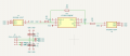
I tried to design a noninverting amplifier circuit for an AC input voltage of about the order of 10 mA to amplify up to the border of 10 V. As the opamp I used the LT1363CS8 with +/- 5 V rails. You can find my KiCAD circuit in the screenshot below. In my ltspice simulation the circuit works properly. But when soldered my opamp output goes directly into negative saturation of -4.1 V. Even if I set my input to ground. This is something I don't really understand at this point.
Thanks for any help since I am kinda new to this. I am happy to provide more information if needed!
 

Attachments

ronsimpson

Joined Oct 7, 2019
4,788
Post your LTspice file.
What is J1 and J3? Are they connectors?
You have very high gain.
Please try moving the input a little below ground, a little above ground. I want to see if it comes off -4.1 to + something.
Pins 1 & 8 are connected to ground. Where did you find information on how to use them?
 
I guess I would start by lowering the feedback resistor down to maybe 200 ohms (gain of 5) and putting in a larger input like 100mV and see if that works first. You should see an output of 500mV. That would verify that your wiring is correct.
 

WBahn

Joined Mar 31, 2012
33,089
I tried to design a noninverting amplifier circuit for an AC input voltage of about the order of 10 mA to amplify up to the border of 10 V. As the opamp I used the LT1363CS8 with +/- 5 V rails. You can find my KiCAD circuit in the screenshot below. In my ltspice simulation the circuit works properly. But when soldered my opamp output goes directly into negative saturation of -4.1 V. Even if I set my input to ground. This is something I don't really understand at this point.
Thanks for any help since I am kinda new to this. I am happy to provide more information if needed!
I assume you mean an input voltage of 10 mV, not mA.

I don't know what you mean by "up to the border of 10 V".

Have you looked at the datasheet for the part? With ±5 V rails, the output voltage swing is only guaranteed to be at least ±3.4 V driving a 150 Ω load. What is the load you are actually driving? What's on the other side of that 30 Ω resistor?

What is the frequency of your signal?

Is it AC coupled?

Have you tried taking it both above and below ground?

As others have said, start with a much tamer gain and see if it works. How it behaves there will provide a lot of insight.

It's hard to make out details on your schematic since you have text on top of text and symbols on top of symbols.

Are you properly bypassing the opamp?
 

Thread Starter

DavidWDenkler

Joined Aug 11, 2026
6
I assume you mean an input voltage of 10 mV, not mA.

I don't know what you mean by "up to the border of 10 V".

Have you looked at the datasheet for the part? With ±5 V rails, the output voltage swing is only guaranteed to be at least ±3.4 V driving a 150 Ω load. What is the load you are actually driving? What's on the other side of that 30 Ω resistor?

What is the frequency of your signal?

Is it AC coupled?

Have you tried taking it both above and below ground?

As others have said, start with a much tamer gain and see if it works. How it behaves there will provide a lot of insight.

It's hard to make out details on your schematic since you have text on top of text and symbols on top of symbols.

Are you properly bypassing the opamp?
Thank you for your quick reply. I will try to answer your questions.

1. The output of my amplifier will drive a piezo from thorlabs (PA4GKH5W).

2. The frequency of my input signal is a few 100 Hz up to very low kHz regime.

3. The circuit is not AC coupled.

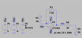
I will try to change the resistance of the feedback resistor to see if that works or not. I also attached my LTSpice simulation.
 

Attachments

Thread Starter

DavidWDenkler

Joined Aug 11, 2026
6
Post your LTspice file.
What is J1 and J3? Are they connectors?
You have very high gain.
Please try moving the input a little below ground, a little above ground. I want to see if it comes off -4.1 to + something.
Pins 1 & 8 are connected to ground. Where did you find information on how to use them?
Thank you for your answer. Yes J1 and J3 are connectors. I attached my LTSpice file here.
 

Attachments

ci139

Joined Jul 11, 2016
2,022
3. The circuit is not *** AC coupled.
☻ -- if it were *** you could set it to auto track the zero // however it'd "hang" at DC input and be frequency dependent then !

☻ the GAIN 150x is quite ambiguous ~vs~ a resulting ±33mV input window is not so impossible to bias into ←← would take a voltage reference (zener) and ±tunable buffer at previous 50Ω resistor's GND-ng point
/// PS! -- the output zero depends on
► input DC bias
► ±Vs
► time passed from power on (mixed with total hours at duty)
► frequency & duty (also as an internal thermal stimulus/driver)
► T° ambient . . .
↑ makes a stable operation more challanging
 

0ri0n

Joined Jan 7, 2025
186
In my ltspice simulation the circuit works properly. But when soldered my opamp output goes directly into negative saturation of -4.1 V.
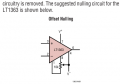
The nulling pins 1/8 are connected to ground. Either leave those open or use the circuit from the datasheet to minimize any DC voltage offset. I doubt that the SPICE model for the LT1363 includes the nulling option.

The op amp (+)-input is also floating in the schematic. Something with a DC path to ground should be connected to it in real life.
 

Thread Starter

DavidWDenkler

Joined Aug 11, 2026
6
The nulling pins 1/8 are connected to ground. Either leave those open or use the circuit from the datasheet to minimize any DC voltage offset. I doubt that the SPICE model for the LT1363 includes the nulling option.

The op amp (+)-input is also floating in the schematic. Something with a DC path to ground should be connected to it in real life.
Yes you are right about the nulling option in the LTSpice model. Is there a way to add this to the model? Otherwise I will try the circuit layout you recommended!
 

Thread Starter

DavidWDenkler

Joined Aug 11, 2026
6
☻ -- if it were *** you could set it to auto track the zero // however it'd "hang" at DC input and be frequency dependent then !

☻ the GAIN 150x is quite ambiguous ~vs~ a resulting ±33mV input window is not so impossible to bias into ←← would take a voltage reference (zener) and ±tunable buffer at previous 50Ω resistor's GND-ng point
/// PS! -- the output zero depends on
► input DC bias
► ±Vs
► time passed from power on (mixed with total hours at duty)
► frequency & duty (also as an internal thermal stimulus/driver)
► T° ambient . . .
↑ makes a stable operation more challanging
Thank you for your answer. Maybe this is my fault but I don't understand everything your mentioned in your answer.
So you say I should AC couple the input of the amplifier?
Can you maybe explain why you proposed the use of the voltage reference at the input with a zener diode?
 

MisterBill2

Joined Jan 23, 2018
28,113
Those of us who do not have that simulator software are not able to see the schematic with the ".asc" file extension. IT IS somehow possible to post the circuit schematic in a format that we can see, though. Many folks use that format instad.
 
One more "detail"!!! If the supply voltages are actually +5 and -5 volts, as stated in post #1, there is no possible way to have an output voltage greater than 5 volts. Not even in theory!!
In addition, considering the very high gain arrangement: 7500/50 =150, you do need to adjust the input offset to ZERO using the input offset adjustment circuit for pins 1 and 8. With a much lower gain it is OK to not adjust the input offset null.
 
Top