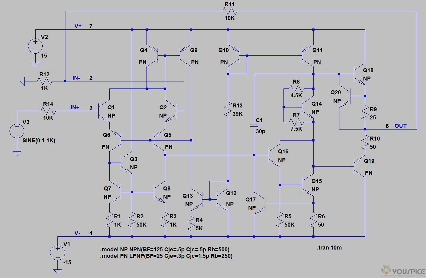
The circuit will try to make the voltage at pin 2 equal to the voltage at pin 3. that would be ground. That drawing is probably the worst hot mess I have ever seen. What is getting amplified is the voltage difference (pin3 - pin 2)
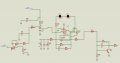
No. That has to be one of the most chaotic, messiest schematic diagrams I've ever seen. If you expect anyone to make a serious attempt at answering your questions, re-draw it NEATLY without running wires to and fro all over the place.
That said, I doubt this circuit will do much of anything at all given the screwball way you've got the 741's balance pins connected.
I think the problem with the wires all over the place on the schematic is because it was drawn with Multisim.
I tidied up the schematic and pointed out the problem with the input offset voltage adjustment pin.
I think the problem with the wires all over the place on the schematic is because it was drawn with Multisim.
I tidied up the schematic and pointed out the problem with the input offset voltage adjustment pin.
The circuit will try to make the voltage at pin 2 equal to the voltage at pin 3. that would be ground. That drawing is probably the worst hot mess I have ever seen. What is getting amplified if the voltabe difference (pin3 - pin 2)
I think the problem with the wires all over the place on the schematic is because it was drawn with Multisim.
I tidied up the schematic and pointed out the problem with the input offset voltage adjustment pin.
There is a mistake in the schematic. The input offset voltage adj pin is connected to pin no.4. But sill the input does not vary and remain stuck at 0.7V.
Sorry 10k is connected between pin 1 and 5. Ok, I'm getting input voltage variation from 0.7-2.7v and output from 6-9.7mV Indeed to change or vary the input from 0.05-0.7mV and o/p from 5.6-6.0mV. what should I change in the circuit?
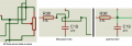
This is the circuit I'm working on....Can you explain how does this circuit work... I/p of the op amp at pin 2 varies from 0.05-0.6V and o/p varies from 5.6mV-6mV at pin 6. What is the output of the transistor??
 Facebook
 Google
 GitHub
 Linkedin
 250.8 KB Views: 69