Facebook
 Google
 GitHub
 Linkedin
I am currently working on the hardware implementation of a Sprott chaotic attractor circuit using analog computation techniques. While the circuit performs correctly in LTspice simulations and produces the expected chaotic attractor trajectories, I have been unable to obtain the expected behavior from the physical hardware implementation. I would greatly appreciate your guidance in identifying the possible causes of the problem.
Project Overview
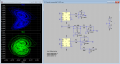
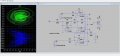
The circuit is based on the Sprott chaotic system realized using analog integrators, summing amplifiers, and nonlinear multiplication blocks. The implementation uses LT1057 operational amplifiers and an AD633 analog multiplier.
In simulation:
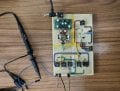
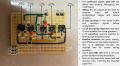
Hardware Implementation
Since I did not have access to a dedicated ±15 V laboratory power supply, I had to generate the required supplies using additional circuitry:
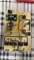
1. Dual Supply Generation
The chaotic circuit requires:
The circuit also requires a fixed -1 V reference.
Since a precision negative reference source was not available, I implemented a separate circuit using:
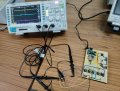
Measurements Performed
The outputs corresponding to:
The expectation was:
I want to implement it on a PCB so that no mistakes are there.
What I Would Like Guidance On
I would be grateful for advice on:
links:
(here he has done lorentz chaotic circuit)
links:
(here he has done lorentz chaotic circuit)
Any guidance regarding likely failure points or recommended debugging steps would be extremely helpful. Please Help me out.
Project Overview
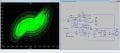
The circuit is based on the Sprott chaotic system realized using analog integrators, summing amplifiers, and nonlinear multiplication blocks. The implementation uses LT1057 operational amplifiers and an AD633 analog multiplier.
In simulation:
- The state variables Vx, Vy, and Vz evolve chaotically.
- Phase portraits such as Vx vs Vy and Vy vs Vz produce the expected butterfly-like chaotic attractor.
- The system remains bounded and exhibits sustained chaotic oscillations.
Hardware Implementation
Since I did not have access to a dedicated ±15 V laboratory power supply, I had to generate the required supplies using additional circuitry:
1. Dual Supply Generation
The chaotic circuit requires:
- +15 V
- -15 V
- A DC-DC boost converter module for generating a higher voltage.
- Additional circuitry to derive the negative rail (-1V).
The circuit also requires a fixed -1 V reference.
Since a precision negative reference source was not available, I implemented a separate circuit using:
- LT431 adjustable reference
- Operational amplifier buffering stage
- Trimmer potentiometer for adjustment
Measurements Performed
The outputs corresponding to:
- Vx
- Vy
- Vz
The expectation was:
- Oscillatory signals on all three state variables
- Chaotic waveforms
- XY plots forming the attractor shape
- Nearly constant DC voltages on some nodes
- Significant noise on the outputs
- No visible chaotic oscillation
- No attractor formation in XY mode
I want to implement it on a PCB so that no mistakes are there.
What I Would Like Guidance On
I would be grateful for advice on:
- A systematic debugging procedure for chaotic analog circuits.
- Which node should be checked first to verify proper operation.
- How to verify whether each integrator stage is functioning correctly.
- Methods to confirm the AD633 multiplier is producing the correct output.
- Whether the custom ±15 V supply arrangement is likely to be the primary issue.
- Whether a PCB implementation is necessary or if this should work reliably on a prototyping board.
- Any recommended measurements that could help isolate the fault.
- LTspice simulation schematics
- Simulation results showing the expected attractor
- Photographs of the completed hardware setup
- Oscilloscope measurements
links:
links:
Any guidance regarding likely failure points or recommended debugging steps would be extremely helpful. Please Help me out.
Attachments
-
 181.3 KB Views: 5
 -
 154.8 KB Views: 7
 -
 218.6 KB Views: 13
 -
 79.7 KB Views: 13
 -
 93.5 KB Views: 13
 -
 812.4 KB Views: 6
 -
 1,016.2 KB Views: 5
 -
 1 MB Views: 4
 -
 731.6 KB Views: 4


")