Facebook
 Google
 GitHub
 Linkedin
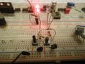
Here's my attempt:
I'm following this configuration:
http://www.allaboutcircuits.com/textbook/experiments/chpt-7/nor-gate-s-r-latch/
I'm trying to recreate a NOR Gate S-R Latch with discrete components instead of using an IC (I don't have the IC and I'd also like to prove these little black box's aren't just magic)... The configuration of the NOT gate part of the NOR gate has it so that the output is actually being driven by the input, with the output only being driven LOW when there is a positive voltage on the middle gate lead... this is problematic because, the LED's I'm using will be fried if I allow any more current through, but the output of the two NOT gates need to be strong enough to drive the corresponding gate but not strong enough to fry the LED... when I drive the corresponding gate with the alternate push button instead of the output of the alternate NOT gate, the NOR gate operates as expected... looking for ideas of how to solve this issue...
Another question I have is if this "hysteresis" phenomenon can be used to "remember" a voltage level with an op amp buffer configuration and a DAC? Have the DAC set a voltage on the buffer, then use a couple of transistors to switch the input to the buffer from the DAC to itself, thereby allowing the DAC to set a specified voltage on some other buffer op amp.