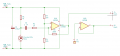
Below is a basic op amp inverter circuit.
Because of the very high internal op amp gain and the negative feedback from output to the (-) input, the op amp output will always try to keep the (-) input essentially equal to the plus input (in this case ground).
This means the (-) input will always be within a few mV of ground (depending upon the actual op amp gain). This is called a virtual ground point.
So when a positive voltage is applied at Vin, a current will flow through R1 to the (-) input.
This starts to raise the voltage at the (-) input, causing the output to go in the negative direction.
To keep the (-) input at the virtual ground, the output voltage must go to a negative value such that the current through R2 is equal to the current through R1.
If the input signal polarity goes negative, then the output goes positive, again to match the current through R1.
Thus the output is inverted from the input with a gain equal to -R2/R1.
The important thing to remember is that, with negative feedback, the output will always try to keep the (-) input within a few mV of the (+) input.
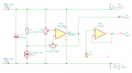
You can use that to see how a non-inverting op amp circuit with gain works also (bottom below) and determine its gain equation.
nice !
for LM(V)358 though, I'd prefer the 'inverting' config, and (+) would be at VCC/2, that is my 'virtual ground', so that voltages would swing about VCC/2. LM358 (without the V) apparently saturates quite early, so i'd guess 'virtual ground' wound need to be lower like VCC/3. LMV358 would likely have less clipping. I'd think.
oh and for lm(v)358, a wacky way to do 'non-inverting' is to daisy chain 2 'inverting' configs (same chip) & u'd get 'non-inverting'?
a strange thinking is if you make (+) VCC/2, and simply connect Vout to Vin (- that is) ! do that give you -1 gain (taking VCC/2 as the virtual ground)?
I'd like to ask an off-topic question about LM358 and such experiments on a breadboard. Do anyone here really patch an op amp on a breadboard for the tests?
Another off-topic LM(V)358 wacky design thinking though.
We can have one variable resistor center tap at (-), the ends connect Vout and Vin. this would be that 'variable gain' resistor. It would likely be 'noisy', a price for all that 'variable gain'.
Then we can have another variable resistor, center tap at (+), the ends connect VCC and GND, this would be that 'adjustable virtual ground'. It is likely to be noisy, though. it is still an inverting amp.
it seemed i'd try this for my electret amp, i'd be able to make do without that coupling capacitor.
or is there any benefit of using that coupling capacitor?
actually i've been thinking about a different design i.e. the coupling capacitor and the feedback resistor literally makes a differentiator amp https://www.allaboutcircuits.com/textbook/semiconductors/chpt-8/differentiator-integrator-circuits/
the math is a little hard to figure out though. i'm kind of thinking if i just use a straight differentiator, what is my gain? lol
(oh maybe i'd need to take Vout = -RC dVin/dt, then i'd need to take my Vin as some kind of VinSin(wt), kind of.
and maybe Vout would be -RC x Vin x w x Cos(wt)?
w=2pixfreq)?
this is kind of interesting in a sense that the gain would be proportional to the *frequency* !
We can have one variable resistor center tap at (-), the ends connect Vout and Vin. this would be that 'variable gain' resistor. It would likely be 'noisy', a price for all that 'variable gain'.
Then we can have another variable resistor, center tap at (+), the ends connect VCC and GND, this would be that 'adjustable virtual ground'. It is likely to be noisy, though. it is still an inverting amp.
Why do you resist posting schematics? It's far easier to read a schematic than a verbal description. There's also less potential for misunderstanding the circuit.
The mess of wires all over a breadboard pickup interference and make seeing what connects to what very difficult so I always soldered parts and a few short jumper wires on stripboard with the copper strips cut to length with a drill bit.
I made hundreds or a few thousand different circuits and they looked and worked so good that most of my prototypes were sold as the custom-made finished product.
Why do you resist posting schematics? It's far easier to read a schematic than a verbal description. There's also less potential for misunderstanding the circuit.
I think the board would look nicer if you aligned the two pots vertically and put them next to each other, put the resistor between RV2 and the opamp, moved the mic down a grid and slid it to the right. You should also put a ceramic cap (10-100nF) near the power pins on the opamp.
thanks dl324, I'd think additional caps would help, but just that they'd add to bom and needs extra pads to connect.
I used a large cap at the power lines which partially alleviated the noise problem, but it didn't really solve it I'd guess.
placing the 2 pot on the side and the mic move might be nice
 Facebook
 Google
 GitHub
 Linkedin
")