Facebook
 Google
 GitHub
 Linkedin
Hello! I have made a PLL design which has an input frequency of 5Mhz and requires an output of 40MHz. Basically the feedback path of the PLL will have to be frequency multiplier of 8.
MY individual blocks of PLL such as PFD, Charge Pump, VCO and frequency divider are working! I have checked them thoroughly. Could anyone help me out who has had previous experience with making a PLL?
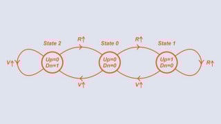
I have individually made each and every block with PMOS and NMOS using 180nm technology! I am attaching picture of the graph and circuit if it helps! I suppose there is an issue with the loop filter can anybody help?


MY individual blocks of PLL such as PFD, Charge Pump, VCO and frequency divider are working! I have checked them thoroughly. Could anyone help me out who has had previous experience with making a PLL?
I have individually made each and every block with PMOS and NMOS using 180nm technology! I am attaching picture of the graph and circuit if it helps! I suppose there is an issue with the loop filter can anybody help?