Need help with ADuM4221A in 13.56MHz RF power amplifier design

ronsimpson

Joined Oct 7, 2019
4,851
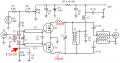
There are many articles in HAM radio for amplifiers built like this. (also, CB radio)
I would remove R6,R1,R2,R4 and put a 2V dc supply there. Adjust this voltage to get the MOSFETs to turn on at the peaks of the input signal.
T2 is a canter tapped primary.
To get started I would remove T3, C4, C5 and just have a secondary on T2. For now use three equal windings.
T1 is 2:1:1 but I would use 1:1:1 to start with.
TL1, TL2, C2, C1 is resonant at 13mhz. But you can leave all that out at first.
Many of us have built this type of amplifier.
1779202257121.png
 

Rf300

Joined Apr 18, 2025
127
The ADuM4221 is absolutely not suitable for a 13.56 MHz operation. It has a propagation delay of up to 44 ns, which is more than half of your 73 ns cycle time. Typical application for those IC's are FET-drivers for PWM in the 100 kHz range and not RF drivers.

There are much more catastrophic bugs in you design: The output filter has an attenuation of about 80 dB @ 13.56 MHz. Cs1 and Cs2 would be a shortcut between D and S of M1/M2 if there were 150 uF capacitors which would act as a capacitor at 13.56 MHz. At this frequency there no capacitors available with this capacitance, btw. they would have an impedance (1/wC) of 78 uOhm at that frequency.

What is the goal of your circuit? Is it a 13.56 MHz RFID/NFC-Transmitter?
 

MisterBill2

Joined Jan 23, 2018
28,490
Based on the first "amplifier" circuit, shown in post #2, I suggest that the TS consult reliable publications from competent sources of HAM RADIO amplifiers intended for the 14 MHZ band to instead be re-designed to operate at 13.56 MHz.
HOWEVER, there remains the issue of legality, at least here in the USA, where redio frequency radiated signals are quite closely regulated.
Of course, I don't recall seeing anycomment about the actual power output level from the proposed circuit, so that might not even be an issue.
 

Rf300

Joined Apr 18, 2025
127
Of course, I don't recall seeing anycomment about the actual power output level from the proposed circuit, so that might not even be an issue.
As mentioned above, at 80 dB attenuation of the output filter, I don't see any problem with the power output level ;)

Additionally 13.56 MHz +- 7 kHz allows a lot of radiated magnetic field strength, in the US (FCC) as well as in Europe (ETSI)
 

ronsimpson

Joined Oct 7, 2019
4,851
13.56 MHz is a frequency primarily used for short-range, low-power wireless communication and industrial, scientific, and medical (ISM) applications.
I think the power amplifier indicates this if for aeronautical mobile communication.
 

0ri0n

Joined Jan 7, 2025
194
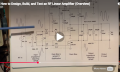
Here is a good place to learn RF power amplifier design. This circuit is much like the one above.
Power amp in LTSPICE Watch this video.
That is a fine example for how to not design a linear amplifier. It works as a "linearized" current mode class-D and not class-AB amplifier. It actually demands a square wave drive. Input side is not well balanced and the lack of magnetical coupling at the output side due to separate chockes make class-AB operation impossible. Output power in the intended "linear" mode of operation is only half of the expected value unless overdriven. With some small mods, as a non-linear class-D amplifier, it would however be perfectly suited for the OP.
 

Thread Starter

Mike2526

Joined Nov 10, 2020
110
There are many articles in HAM radio for amplifiers built like this. (also, CB radio)
I would remove R6,R1,R2,R4 and put a 2V dc supply there. Adjust this voltage to get the MOSFETs to turn on at the peaks of the input signal.
T2 is a canter tapped primary.
To get started I would remove T3, C4, C5 and just have a secondary on T2. For now use three equal windings.
T1 is 2:1:1 but I would use 1:1:1 to start with.
TL1, TL2, C2, C1 is resonant at 13mhz. But you can leave all that out at first.
Many of us have built this type of amplifier.
View attachment 367417


Dear ronsimpson,

Thank you so much for your detailed response. You are right, it is a good example. However, I am not very good at designing transformers in LTspice. Also, I prefer to avoid using multiple transformers in one circuit, which is why I designed the Class DE PA. Even though I have used one coupling transformer at the output, it works well. So, is there any modification possible in my current design, as I have shown in my previous posts?

Thank you again for your guidance.
 

Thread Starter

Mike2526

Joined Nov 10, 2020
110
The ADuM4221 is absolutely not suitable for a 13.56 MHz operation. It has a propagation delay of up to 44 ns, which is more than half of your 73 ns cycle time. Typical application for those IC's are FET-drivers for PWM in the 100 kHz range and not RF drivers.

There are much more catastrophic bugs in you design: The output filter has an attenuation of about 80 dB @ 13.56 MHz. Cs1 and Cs2 would be a shortcut between D and S of M1/M2 if there were 150 uF capacitors which would act as a capacitor at 13.56 MHz. At this frequency there no capacitors available with this capacitance, btw. they would have an impedance (1/wC) of 78 uOhm at that frequency.

What is the goal of your circuit? Is it a 13.56 MHz RFID/NFC-Transmitter?


Dear Rf300,

Thank you so much for your kind reply and suggestions. Below is my point of view on why I chose the ADuM4221.

The designed PA operates at 13.56 MHz, targeting the ISM (Industrial, Scientific, and Medical) band for biomedical wireless power transfer (WPT) applications, such as wearable medical devices.

The ADuM4221 is an isolated half‑bridge gate driver that uses iCoupler technology. It provides independent and isolated high‑side and low‑side outputs with 5700 V rms true galvanic isolation. It is the only IC from your list that simultaneously offers:

Built-in half‑bridge (one IC drives both M1 and M2)
True galvanic isolation (critical for biomedical applications)
Adjustable dead time (no external RC network needed)
4 A peak output current (sufficient to drive IRF510 gates at 13.56 MHz)
Output supply up to 35 V (compatible with our +12 V gate drive rail)
Dual inputs (VIA and VIB) that accept separate 0° and 180° signals directly from Q2/Q3

The galvanic isolation is a significant advantage over the IR2110 for biomedical applications, as it prevents ground loops between the power stage and any patient‑connected circuitry.

The ADuM4221 provides true galvanic isolation using iCoupler chip‑scale transformer technology. Each output channel is independently isolated, eliminating the need for a bootstrap circuit on the high side in many configurations. GNDA floats with the VSW node automatically, and VDDA supplies the high‑side driver from an isolated +12 V rail.
 

Thread Starter

Mike2526

Joined Nov 10, 2020
110
Based on the first "amplifier" circuit, shown in post #2, I suggest that the TS consult reliable publications from competent sources of HAM RADIO amplifiers intended for the 14 MHZ band to instead be re-designed to operate at 13.56 MHz.
HOWEVER, there remains the issue of legality, at least here in the USA, where redio frequency radiated signals are quite closely regulated.
Of course, I don't recall seeing anycomment about the actual power output level from the proposed circuit, so that might not even be an issue.

Dear MisterBill2,

The designed PA operates at 13.56 MHz, targeting the ISM (Industrial, Scientific, and Medical) band for biomedical wireless power transfer (WPT) applications, such as wearable medical devices. No other purpose.
 

Thread Starter

Mike2526

Joined Nov 10, 2020
110
13.56 MHz is a frequency primarily used for short-range, low-power wireless communication and industrial, scientific, and medical (ISM) applications.
I think the power amplifier indicates this if for aeronautical mobile communication.

The designed PA operates at 13.56 MHz, targeting the ISM (Industrial, Scientific, and Medical) band for biomedical wireless power transfer (WPT) applications, such as wearable medical devices. The ouptput power can be 1W ~ 2W. So we can say it is used for short-range communication.
 

Rf300

Joined Apr 18, 2025
127
If you are talking about only 1 ... 2 W output power, your design is real overkill. Have you thought about cheap RFID-Reader-ICs available from different manufacturers (TI, NXP, ST, ...)? They work at 13.56 MHz and can deliver an output power of up to 2 W. And the big advantage: they are designed to work at 13.56 MHz, whereas the ADuM4221 isn't.

Take some optocouplers which are specified for your safety ratings for isolating the communication interface, if necessary, and that's it.
 

Thread Starter

Mike2526

Joined Nov 10, 2020
110
If you are talking about only 1 ... 2 W output power, your design is real overkill. Have you thought about cheap RFID-Reader-ICs available from different manufacturers (TI, NXP, ST, ...)? They work at 13.56 MHz and can deliver an output power of up to 2 W. And the big advantage: they are designed to work at 13.56 MHz, whereas the ADuM4221 isn't.

Take some optocouplers which are specified for your safety ratings for isolating the communication interface, if necessary, and that's it.


Dear Rf300,

Thank you very much for your suggestions. I am interested in designing a Class DE power amplifier. Later, I plan to increase the output power to about 5W–7W for biomedical wireless power transfer (WPT) applications. Therefore, I would prefer not to change my current design completely. However, I am open to adopting a different design if needed, as I am unsure where the fault lies. Could you please suggest what I need to change, where the error might be, and how I can improve my design strategy?

I would be truly grateful for any assistance you or others in the group can provide.
 

Thread Starter

Mike2526

Joined Nov 10, 2020
110
Dear all,
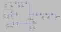
I am working on an RF power amplifier designed to operate at 13.56 MHz. I am using the ADuM4221A gate driver IC in my circuit. The issue I am facing is that the output signal from the driver is not correct. More importantly, even the input signals at pins VIA and VIB are not as expected. According to the datasheet and my understanding, these two input signals should be 180 degrees out of phase with each other (with the same magnitude). However, after running the simulation in LTspice, I am not getting the required phase relationship (also, the magnitude is different). I have attached my .asc file (in the previous post, Post #5) for your reference. I would be very grateful if any of the experienced members in this group could kindly take a look at my circuit and guide me on what might be going wrong. Thank you very much in advance for your time and help
 

MisterBill2

Joined Jan 23, 2018
28,490
Dear MisterBill2,

The designed PA operates at 13.56 MHz, targeting the ISM (Industrial, Scientific, and Medical) band for biomedical wireless power transfer (WPT) applications, such as wearable medical devices. No other purpose.
Consider that even when RF radiated emissions are legal and allowed THEY ARE STILL REGULATED! I did not investigate the power output of the amplifier shown, but even in the bands where assorted emissions are permitted, they are still regulated. That means that the emissions must not interfere with other services.
 

Rf300

Joined Apr 18, 2025
127
Therefore, I would prefer not to change my current design completely. However, I am open to adopting a different design if needed, as I am unsure where the fault lies. Could you please suggest what I need to change, where the error might be, and how I can improve my design strategy?
As already mentioned, the biggest error in your design is the ADuM4221. It is simply too slow for 13.56 MHz. The next error is the selection of IRF510. This MOSFET is much too big for an output power of max. 7 W. You don't need V_DSmax of 100 V and I_Dmax of 5.6 A for only 7 W. So in my opinion your concept is totally wrong. Use a smaller FET, which can be driven directly from a 5 V logic level crystal oscillator. Look at the design principles of a pure class E Amplifier, this could be a good first step. But depending on your load for the WPT the tuning of a class E amplifier is somehow tricky, especially if your load is resonant in the freqency range around 13.56 MHz.

The next big error in your design is your output filter. As I already mentioned, this filter has an attenuation of about 80 dB(!!!) at 13.56 MHz. Do a short LTspice simulation to see that this is the bad truth. This means: nothing of your generated transmission power will ever arrive at the transmission antenna.

One other aspect came into my mind. Your goal is to transmit up to 7 W of RF into human tissue. Depending on the antenna size, I am afraid this could cause problems with regulation standards for human exposure to radiated RF. Did you think about it?
 

Thread Starter

Mike2526

Joined Nov 10, 2020
110
As already mentioned, the biggest error in your design is the ADuM4221. It is simply too slow for 13.56 MHz. The next error is the selection of IRF510. This MOSFET is much too big for an output power of max. 7 W. You don't need V_DSmax of 100 V and I_Dmax of 5.6 A for only 7 W. So in my opinion your concept is totally wrong. Use a smaller FET, which can be driven directly from a 5 V logic level crystal oscillator. Look at the design principles of a pure class E Amplifier, this could be a good first step. But depending on your load for the WPT the tuning of a class E amplifier is somehow tricky, especially if your load is resonant in the freqency range around 13.56 MHz.

The next big error in your design is your output filter. As I already mentioned, this filter has an attenuation of about 80 dB(!!!) at 13.56 MHz. Do a short LTspice simulation to see that this is the bad truth. This means: nothing of your generated transmission power will ever arrive at the transmission antenna.

One other aspect came into my mind. Your goal is to transmit up to 7 W of RF into human tissue. Depending on the antenna size, I am afraid this could cause problems with regulation standards for human exposure to radiated RF. Did you think about it?

Dear Rf300,

Thank you very much for your detailed message. I understand your point, and I agree with you. As you know, I posted my query seeking help from the community. In this regard, could you kindly share a circuit or topology for a Class DE or Class E amplifier? Such an example would greatly help me build a stronger understanding of this area.

You are an expert in this domain, but as a beginner, I find it a bit challenging. If you do not mind and could spare some time from your busy schedule, I would truly appreciate your guidance in helping me build the amplifier as described. Thank you once again for your kindness and support.
 

Rf300

Joined Apr 18, 2025
127
Here is a schematic of a 13.56 MHz RFID transmitter which can deliver about 2 W into 50 Ohms. M1/M2 are 2 FETs in an SO8 housing. You can increase the output power by increasing V1. You might adjust the voltage divider R4/R5 to get an optimum DC-bias for the FETs. This design is a good starting point. Depending on the parameters of your output filter inductors (parasitic resistance, parasitic mutual inductance due to positioning of L3 ... L5, etc.) there may be additional tuning necessary. Maybe it will be necessary to add more FETs in parallel if you need more power. For V3 you can use a CMOS crystal oscillator, perhaps is some buffering with some 74AHC125 in parallel necessary. If you drive the FETs with a 5 V oscillator, DC-bias adjustment is needed. Depending on your tuning and layout an additional filtering of harmonics, especially 27.12 MHz and 40.68 MHz might be necessary.
Transmitter.png
 

Thread Starter

Mike2526

Joined Nov 10, 2020
110
Here is a schematic of a 13.56 MHz RFID transmitter which can deliver about 2 W into 50 Ohms. M1/M2 are 2 FETs in an SO8 housing. You can increase the output power by increasing V1. You might adjust the voltage divider R4/R5 to get an optimum DC-bias for the FETs. This design is a good starting point. Depending on the parameters of your output filter inductors (parasitic resistance, parasitic mutual inductance due to positioning of L3 ... L5, etc.) there may be additional tuning necessary. Maybe it will be necessary to add more FETs in parallel if you need more power. For V3 you can use a CMOS crystal oscillator, perhaps is some buffering with some 74AHC125 in parallel necessary. If you drive the FETs with a 5 V oscillator, DC-bias adjustment is needed. Depending on your tuning and layout an additional filtering of harmonics, especially 27.12 MHz and 40.68 MHz might be necessary.
View attachment 367551

Thank you very much for your kind help. I will redraw the circuit in LTspice and implement the changes as you recommended. Should any further questions arise during this process, I will reach out to you again. I am confident that I will be able to proceed effectively, following the guidance you have provided. Once again, I sincerely appreciate your valuable help and support.
 
Top