Facebook
 Google
 GitHub
 Linkedin
Dears,
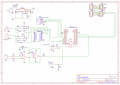
since i,m new in pcb designing ,i have make a schematic using easyeda (that was easy) but making the pcb is a nightmare,15 days trying i was able to make 70% and now im stuck,the auto router do not help.
kindly if any one can help?
Thanks
since i,m new in pcb designing ,i have make a schematic using easyeda (that was easy) but making the pcb is a nightmare,15 days trying i was able to make 70% and now im stuck,the auto router do not help.
kindly if any one can help?
Thanks
Attachments
-
43.7 KB Views: 7
-
156.3 KB Views: 4